Build guide for SAMODULAR's 259 DIY module
Disclaimer
The PCBs are sold unpopulated and need to be stuffed by yourself. Advanced electronic skills are needed to build this module.
You can follow this build guide to build your own 259s DIY module but please note that we will not take any responsibility for damages or injuries when building and running this module.
Thank you for your understanding.
Caution
This DIY module build requires you to solder a lot of components. Please note that solder fume can cause serious damage to your health.
Please do NOT solder without a fume extractor or at least ventilation that prevents breathing toxic solder fumes. If you have ever cleaned a fume extractor filter you will never ever again solder without fume extraction or at least proper ventilation.
Stay safe !
Introduction
Thank you for purchasing SAMODULAR’s 259s PCBs.
This guide will help you building the 259s CWG. The PCBs come with additional soldermask and silkscreened reference designator though to make you life easier.
The soldermask will prevent you from bridging 2 nearby pads when soldering for example and it will also prevent any corrosion when you work in environments with high humidity.
The silkscreened reference designator on the other hand will make it super easy to find the right spots for all components to be soldered.
Now lets have fun – happy building !
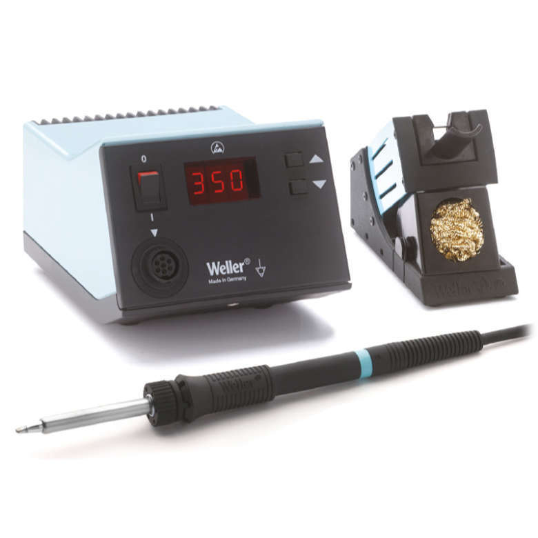
The right tools
In this build I have used the following tools. Those are just suggestions and you can sure use whatever you are used to.


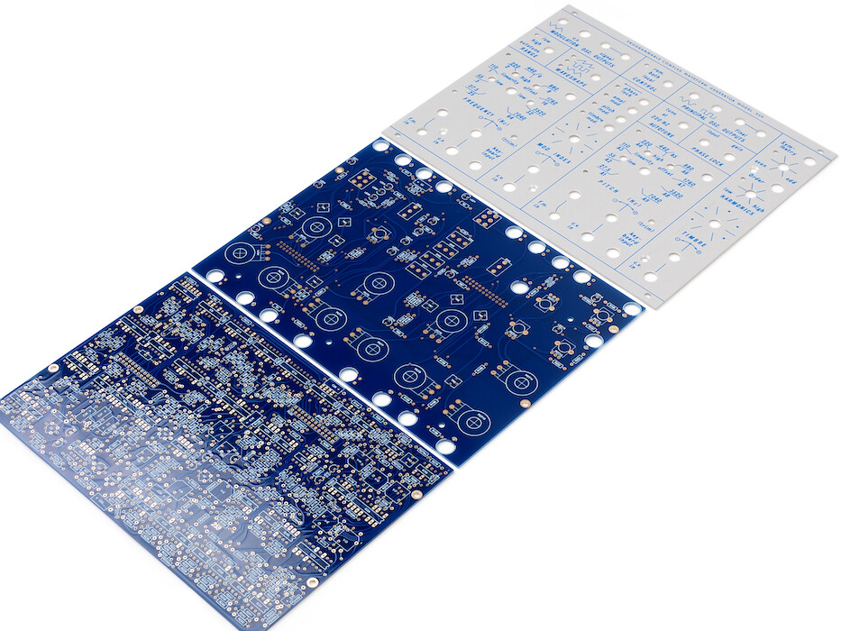
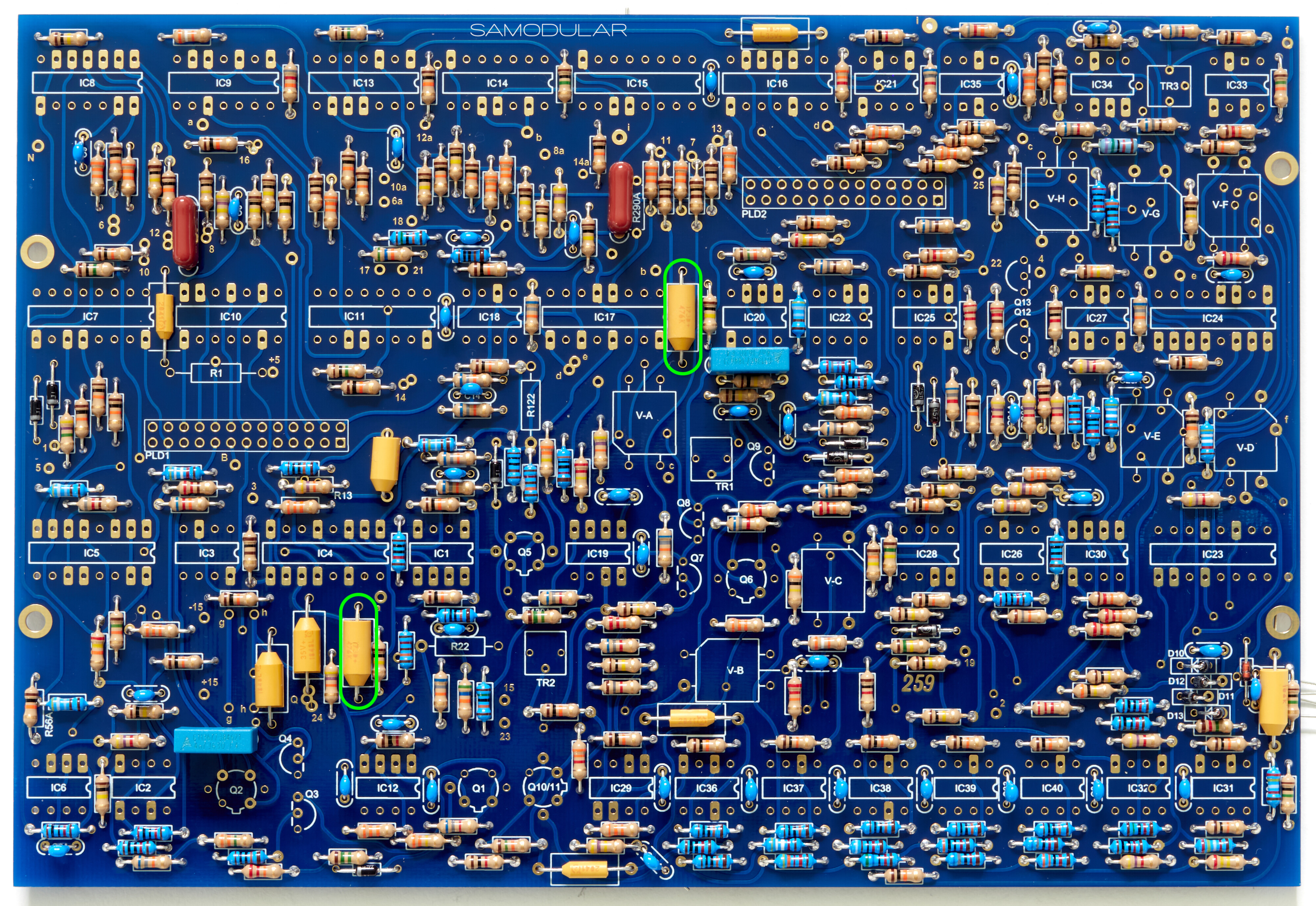
Part 1 – PCB2
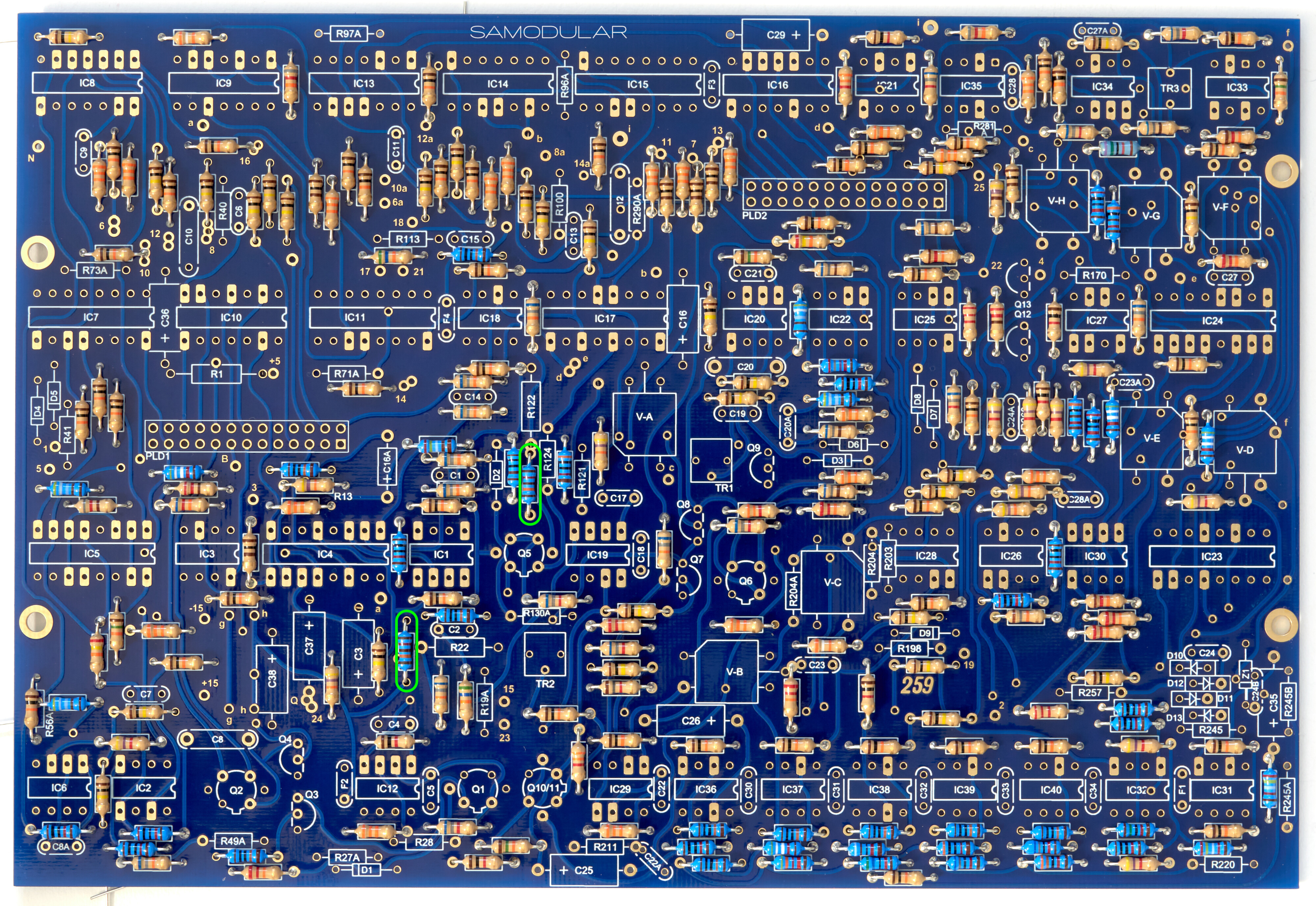
Placing diodes & resistors (100R – 10K)
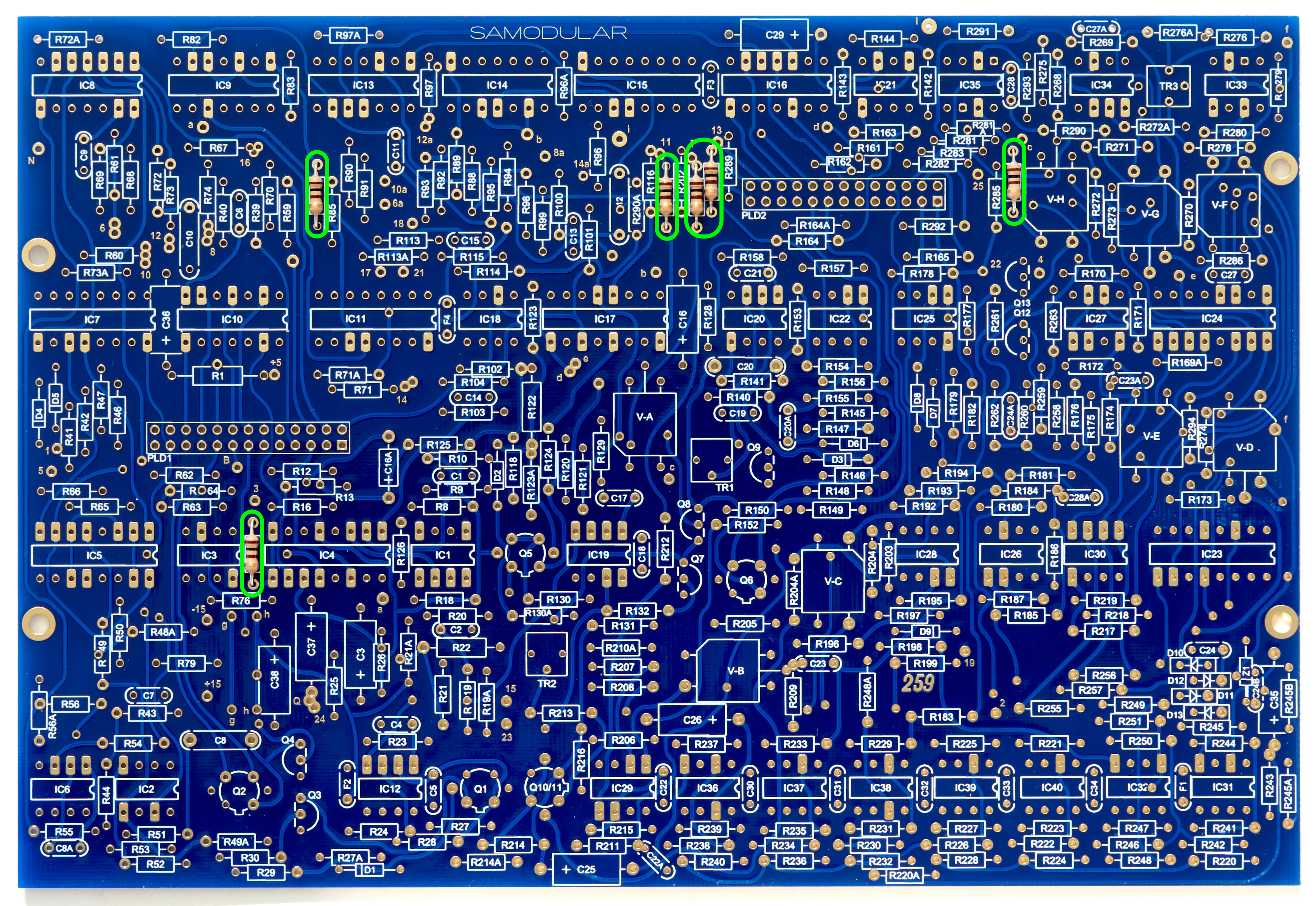
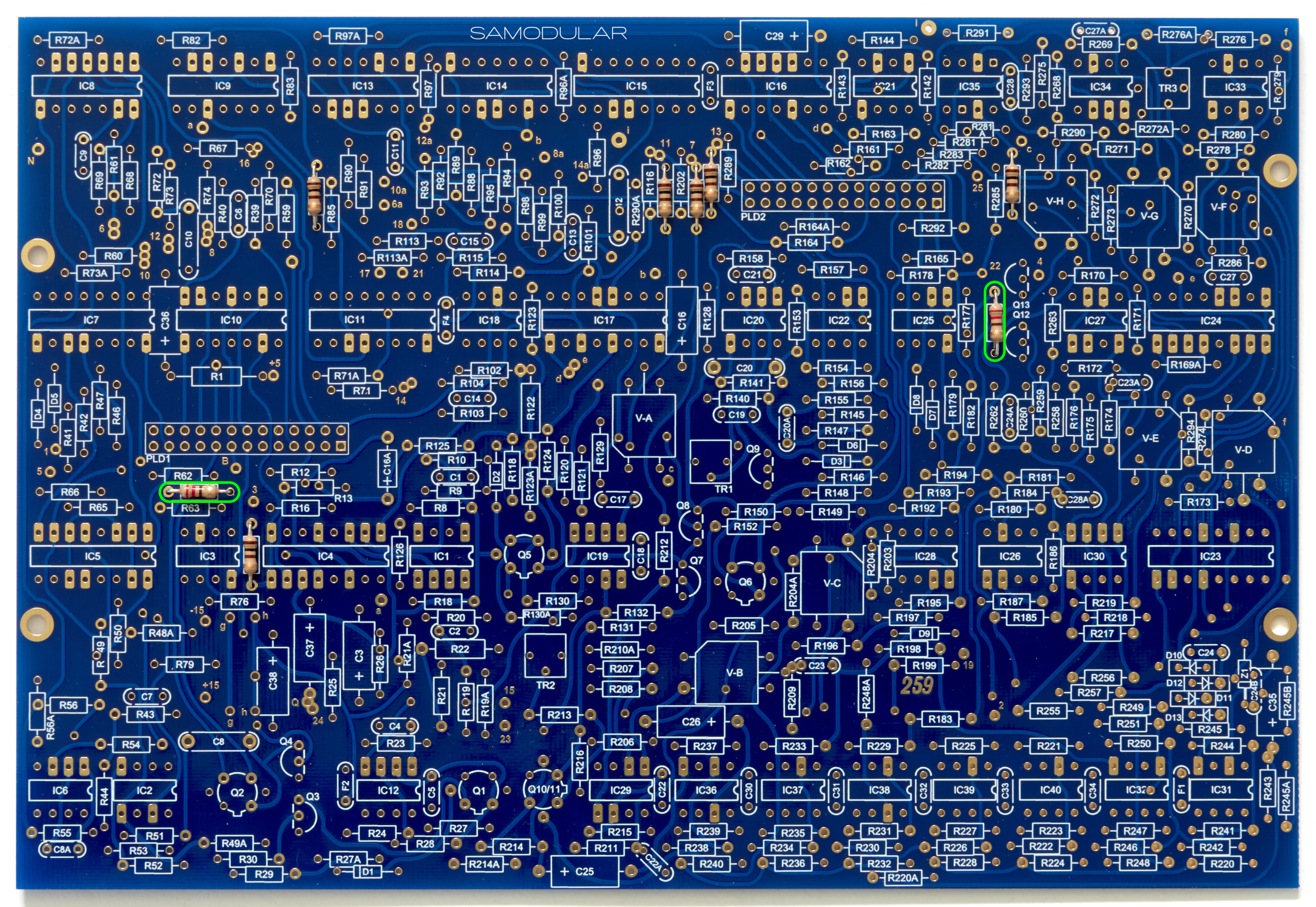
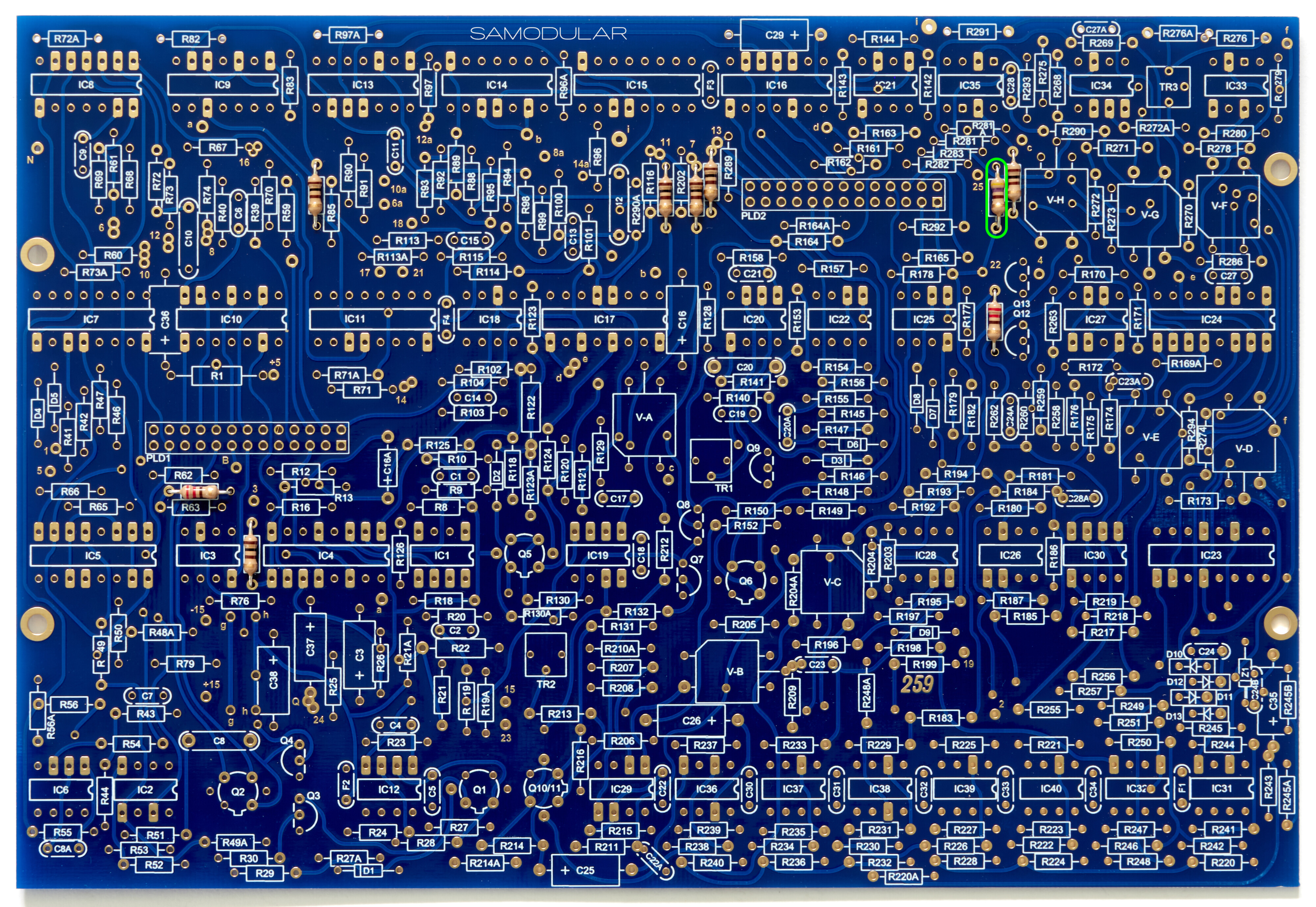
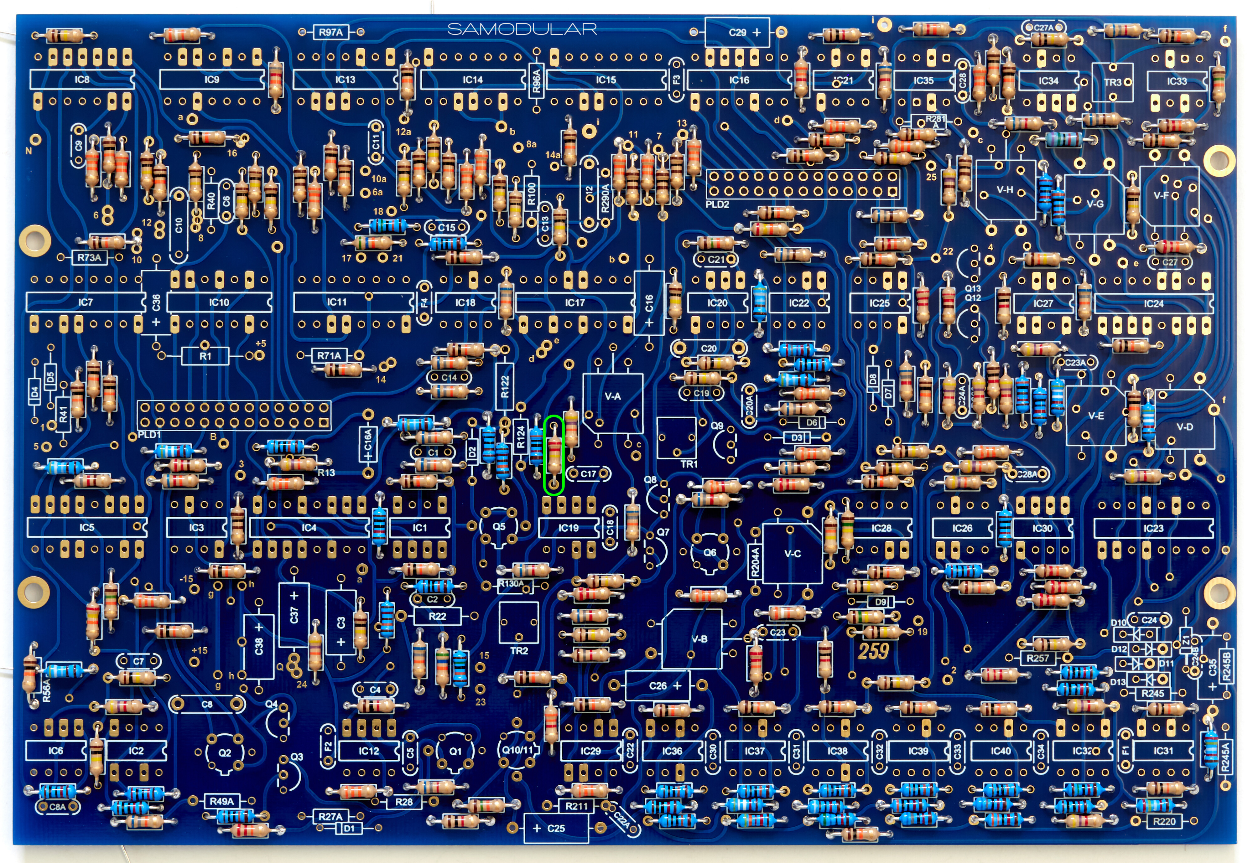
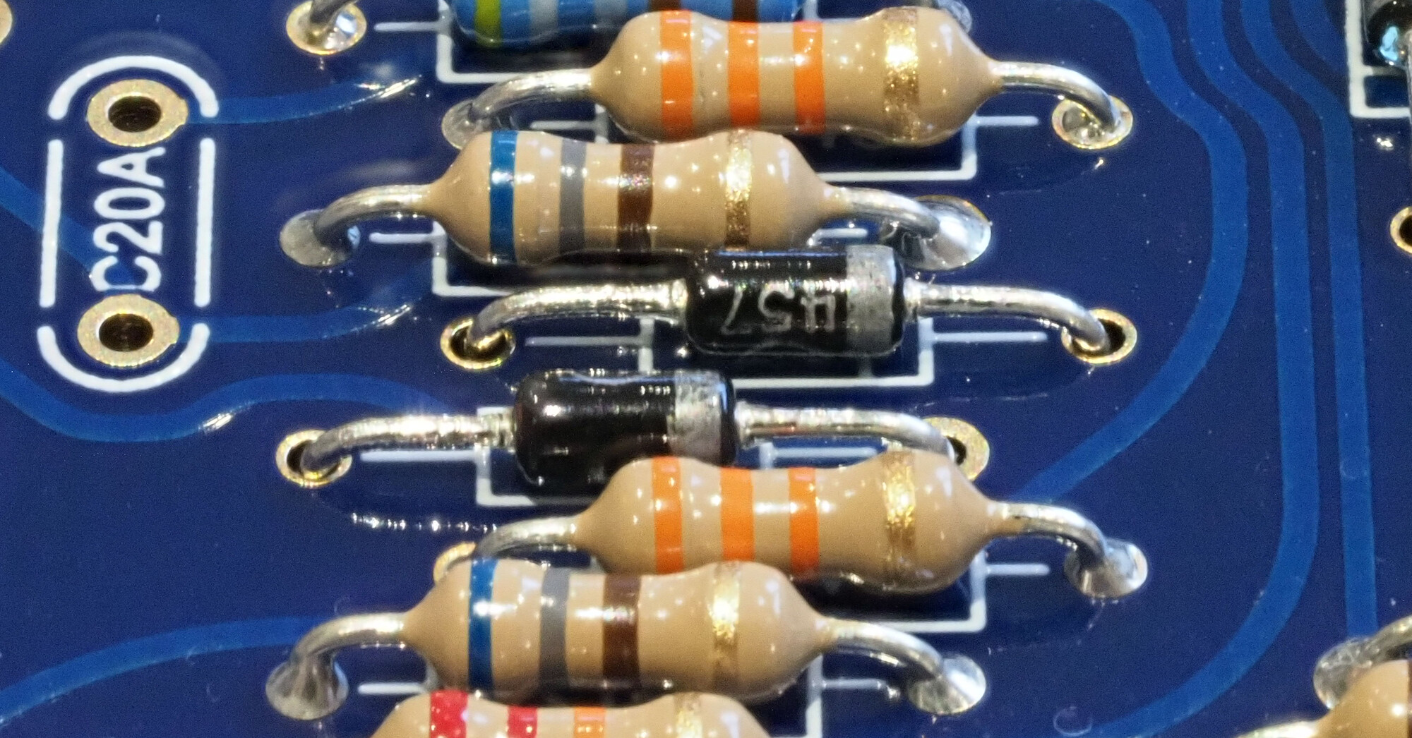
The 259s build uses different lead spacings for the components. Before placing a diode or resistor check the lead spacing before bending the legs of those parts. For diodes about 4mm legth from the body should be fine. Bend carbon resistor legs (brown) about 2mm away from their body and for most metal resistors 5mm should be fine. Again – please check before bending the leads.
Once you have seated a component – press it with one finger against the PCB and bend the leads on the other side. This will hold the component in place until it is soldered to the PCB.
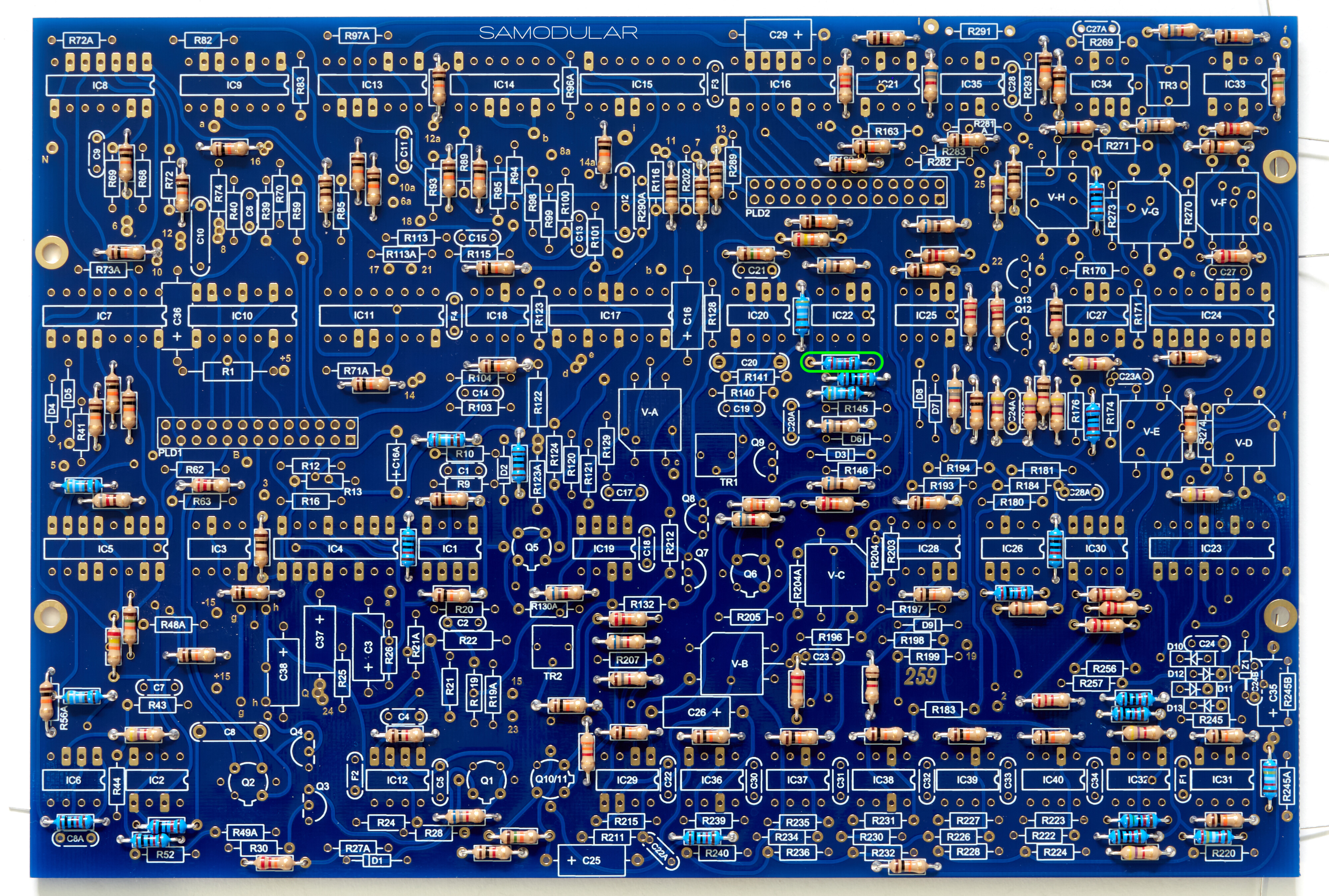
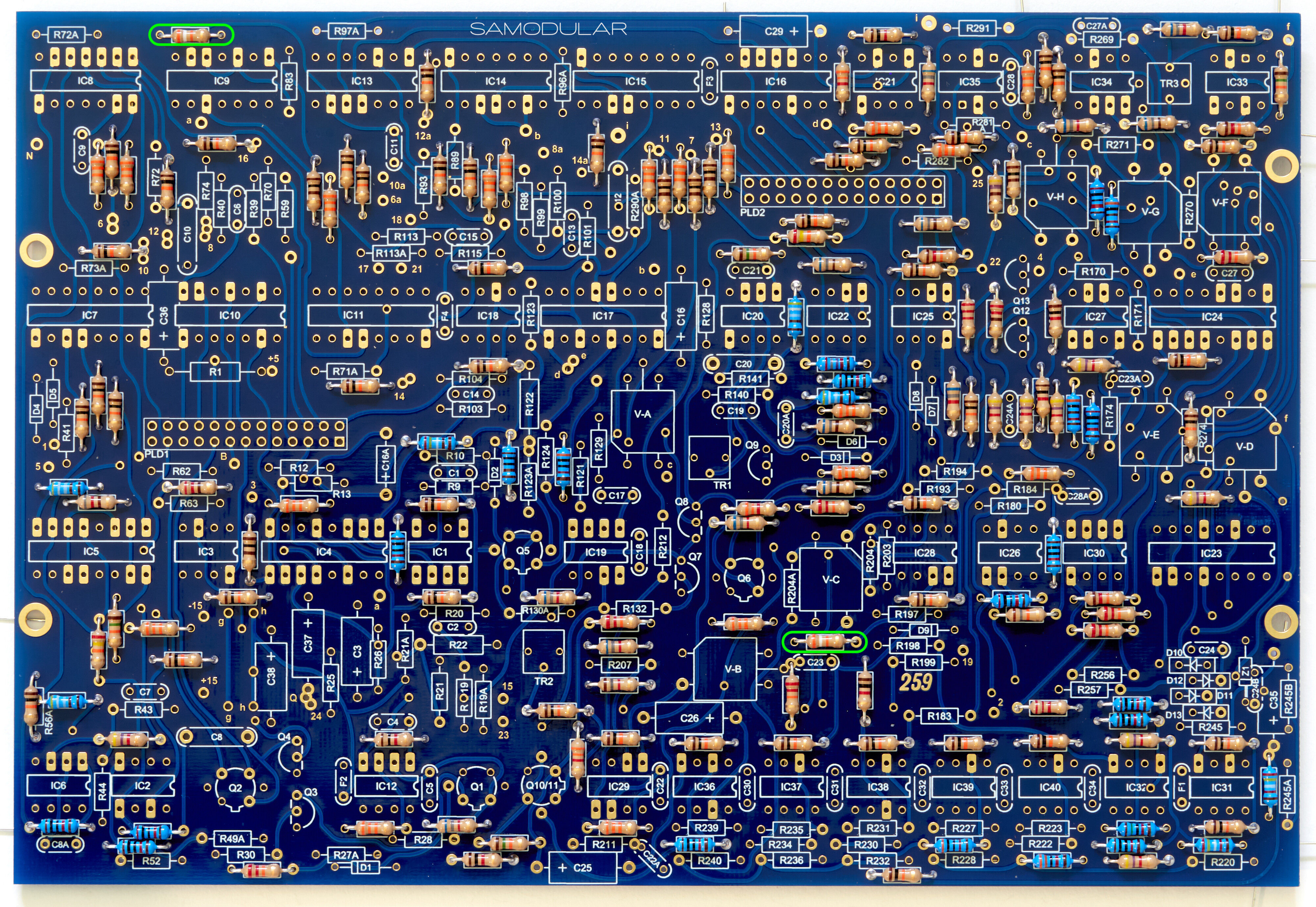
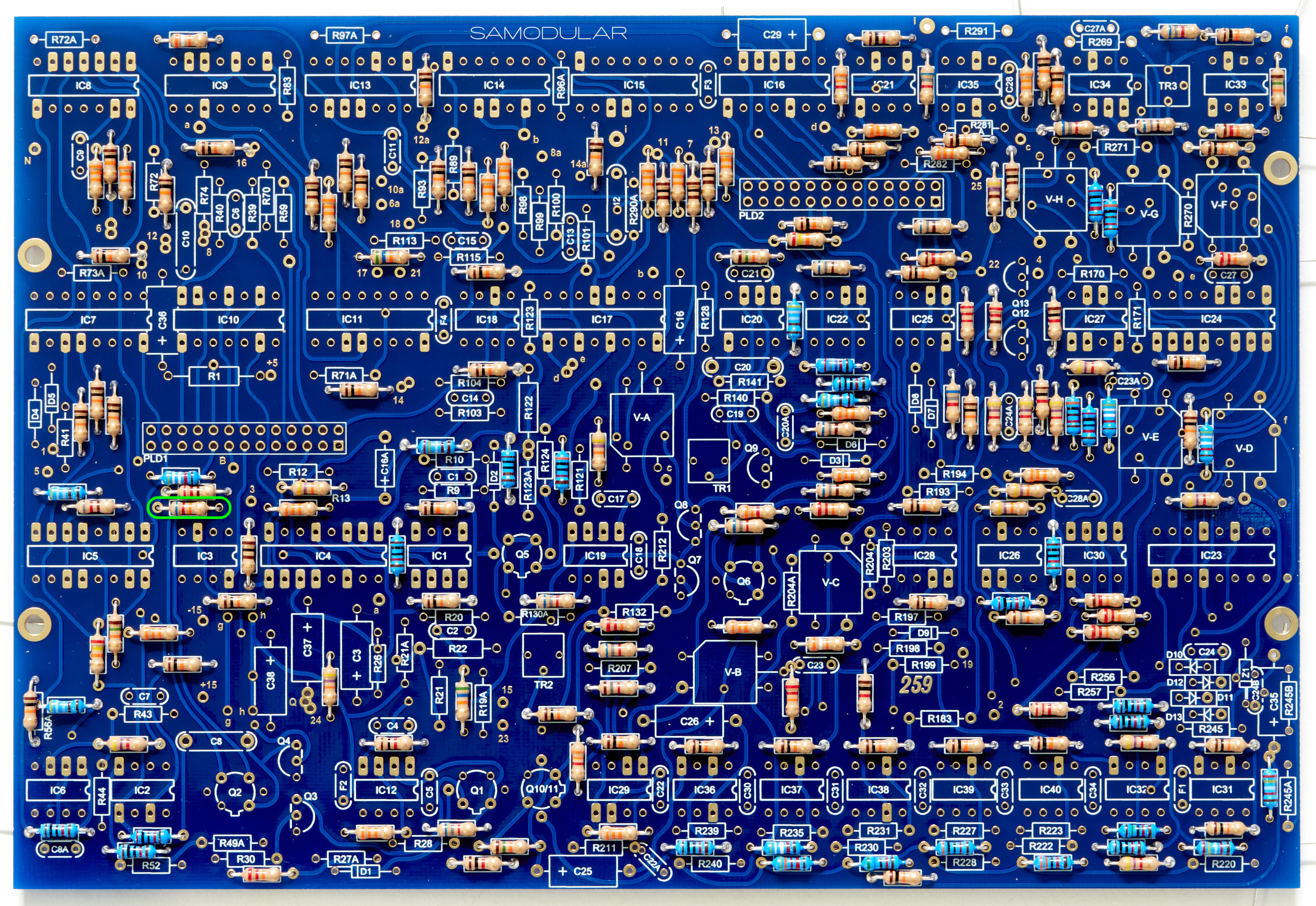
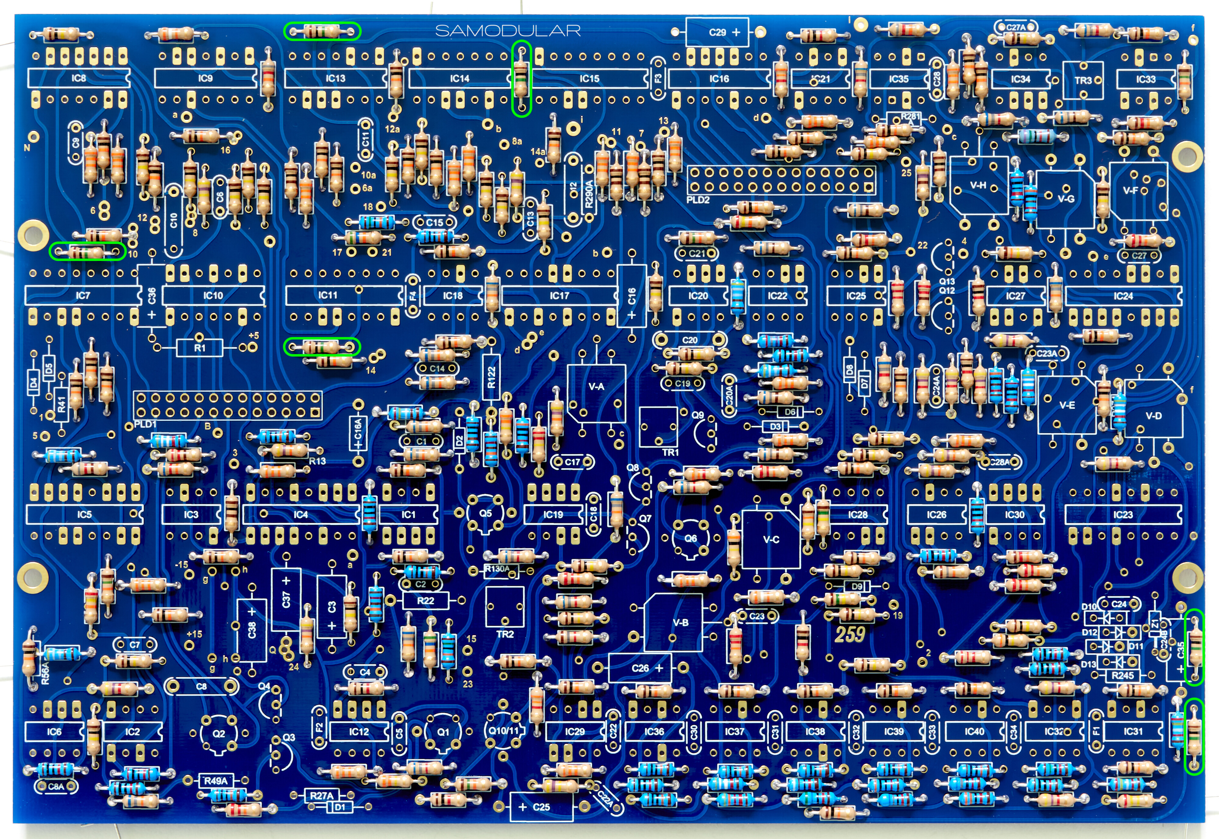
To make life a bit easier I made pictures after installing all parts of a specific value so you basically have an easy to follow parts placement map. In “Part 1” of this guide I started with the 1N457 diodes all the way up to 10K resistors. In most of my builds I start pupulating PCBs with the most flat parts. This way you can put the PCB on a flat desk and the components will be pushed against the board while soldering.
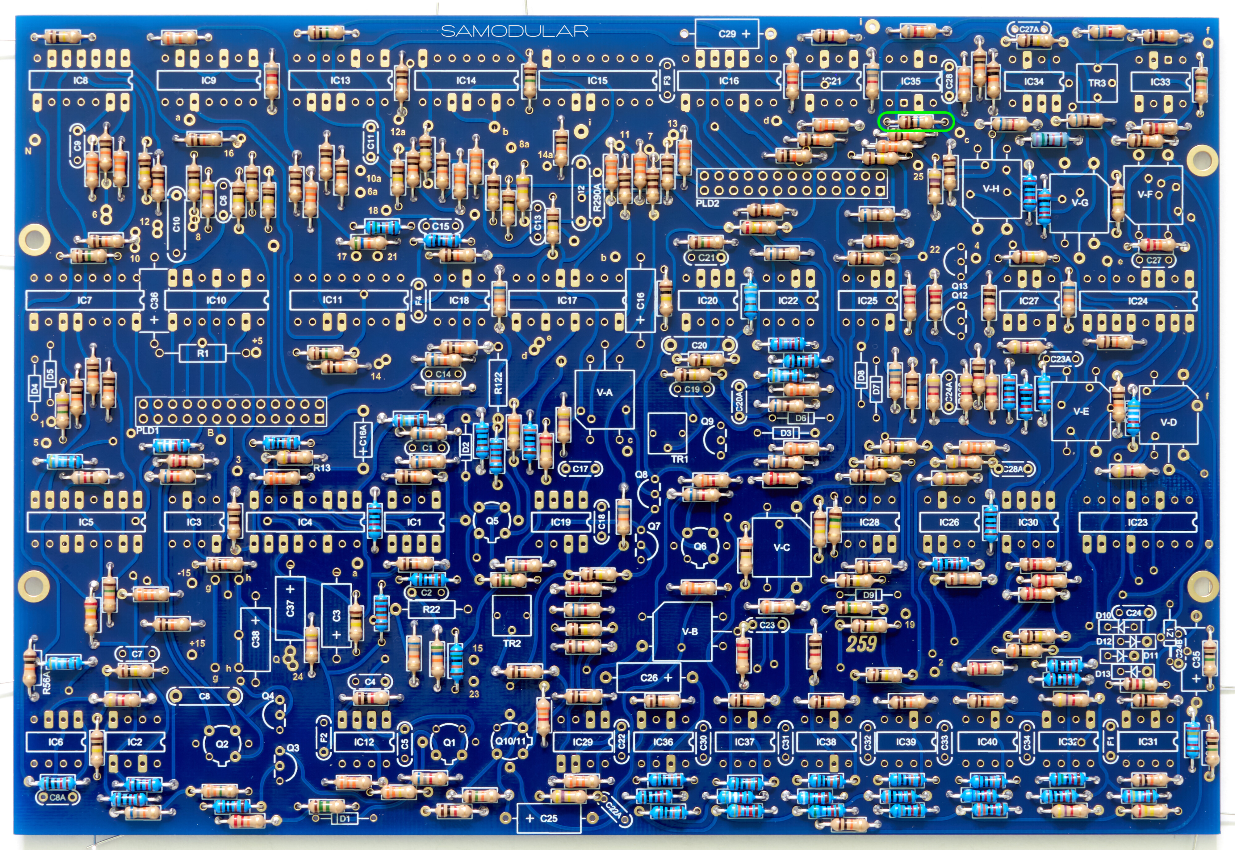
Click on the thumbnails below for high resolution images.


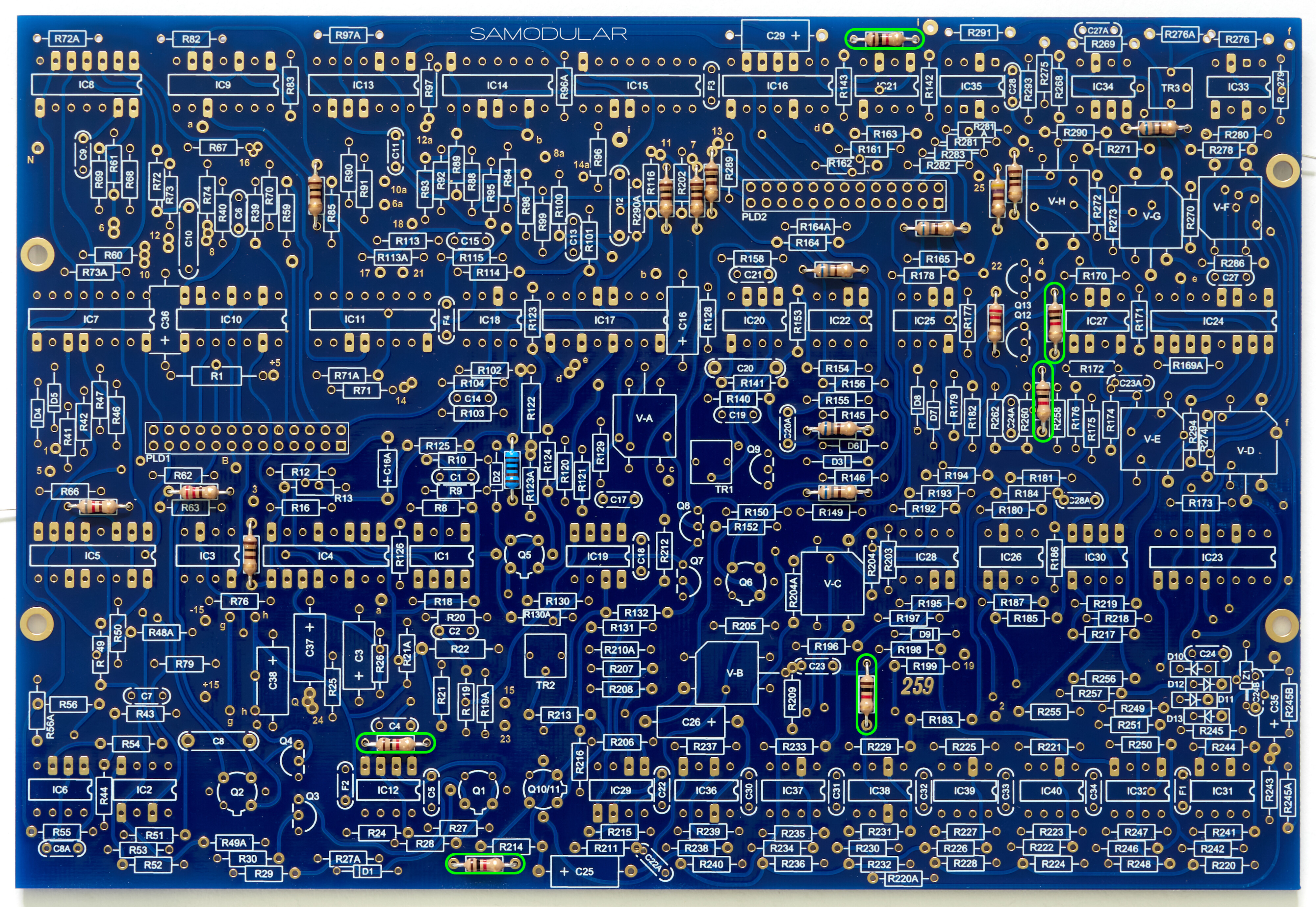

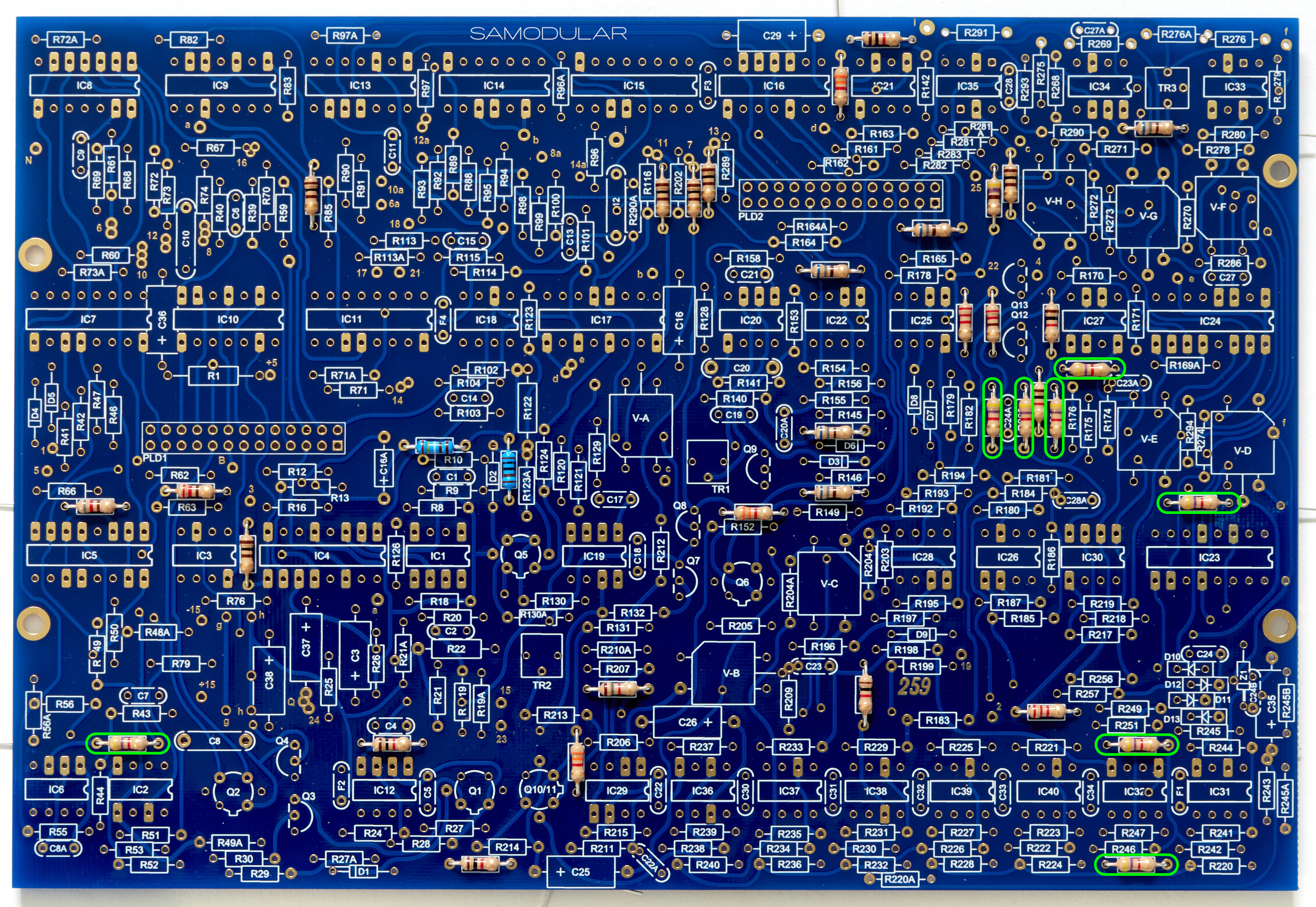


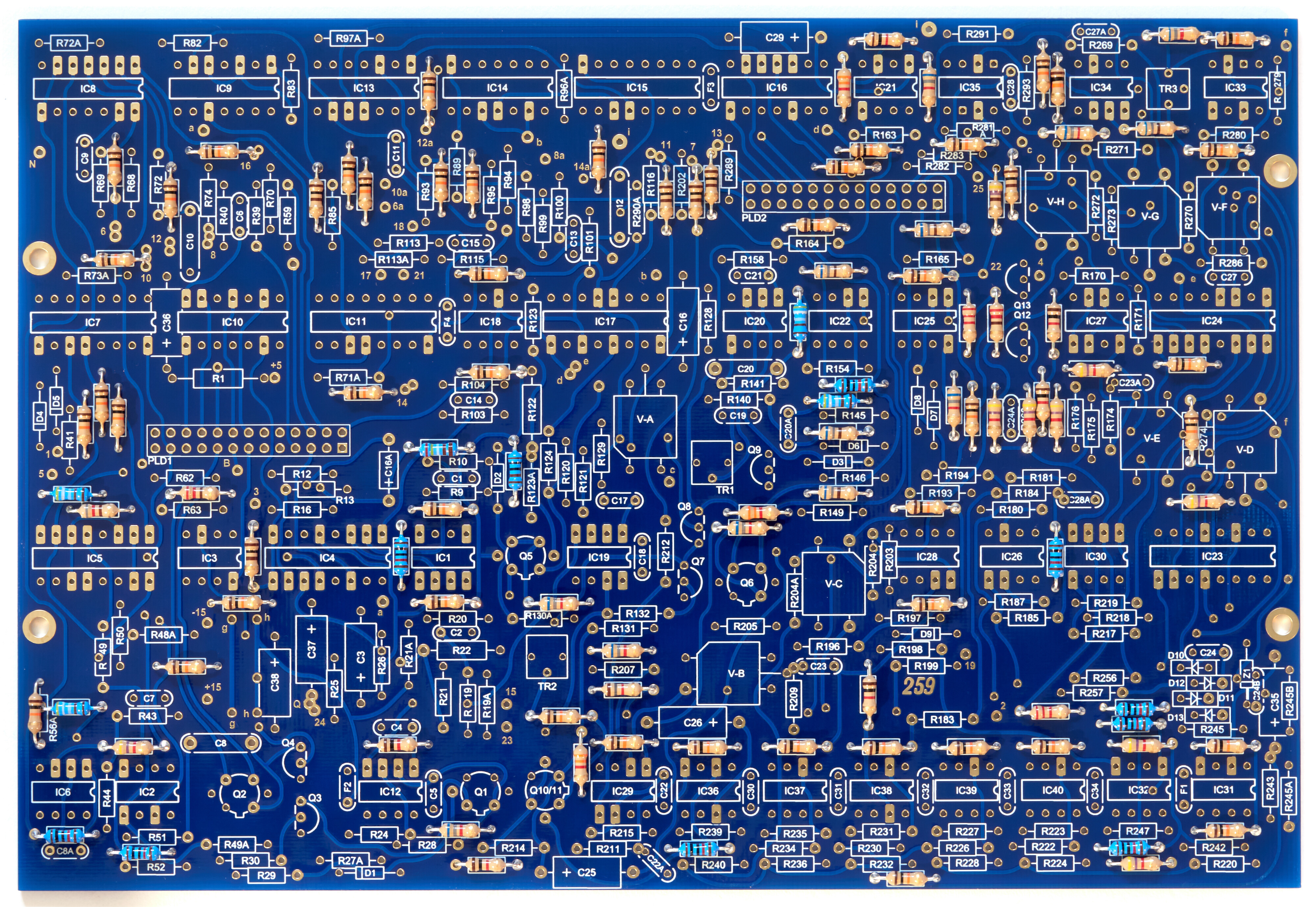
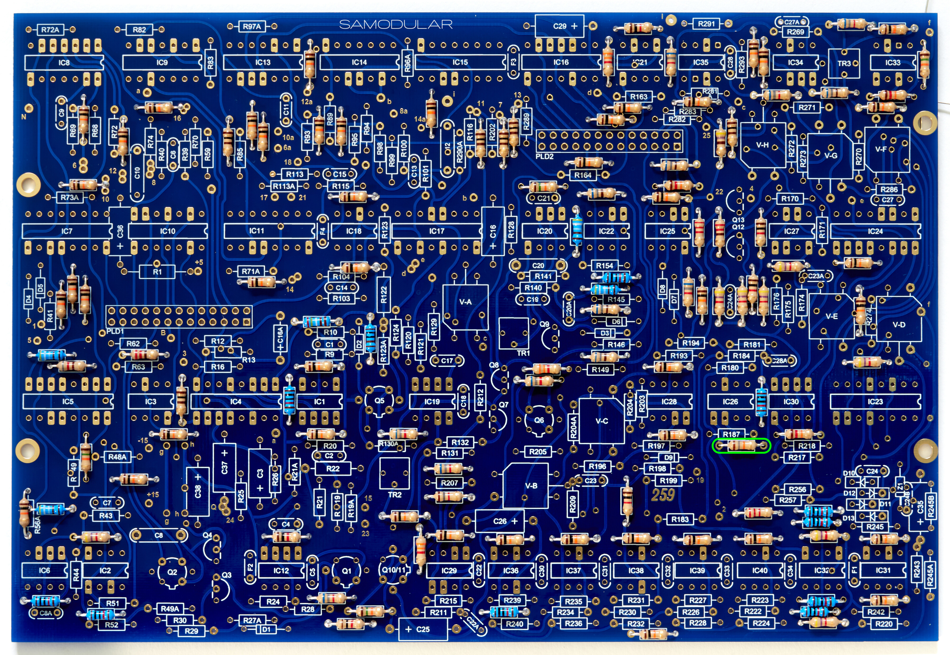
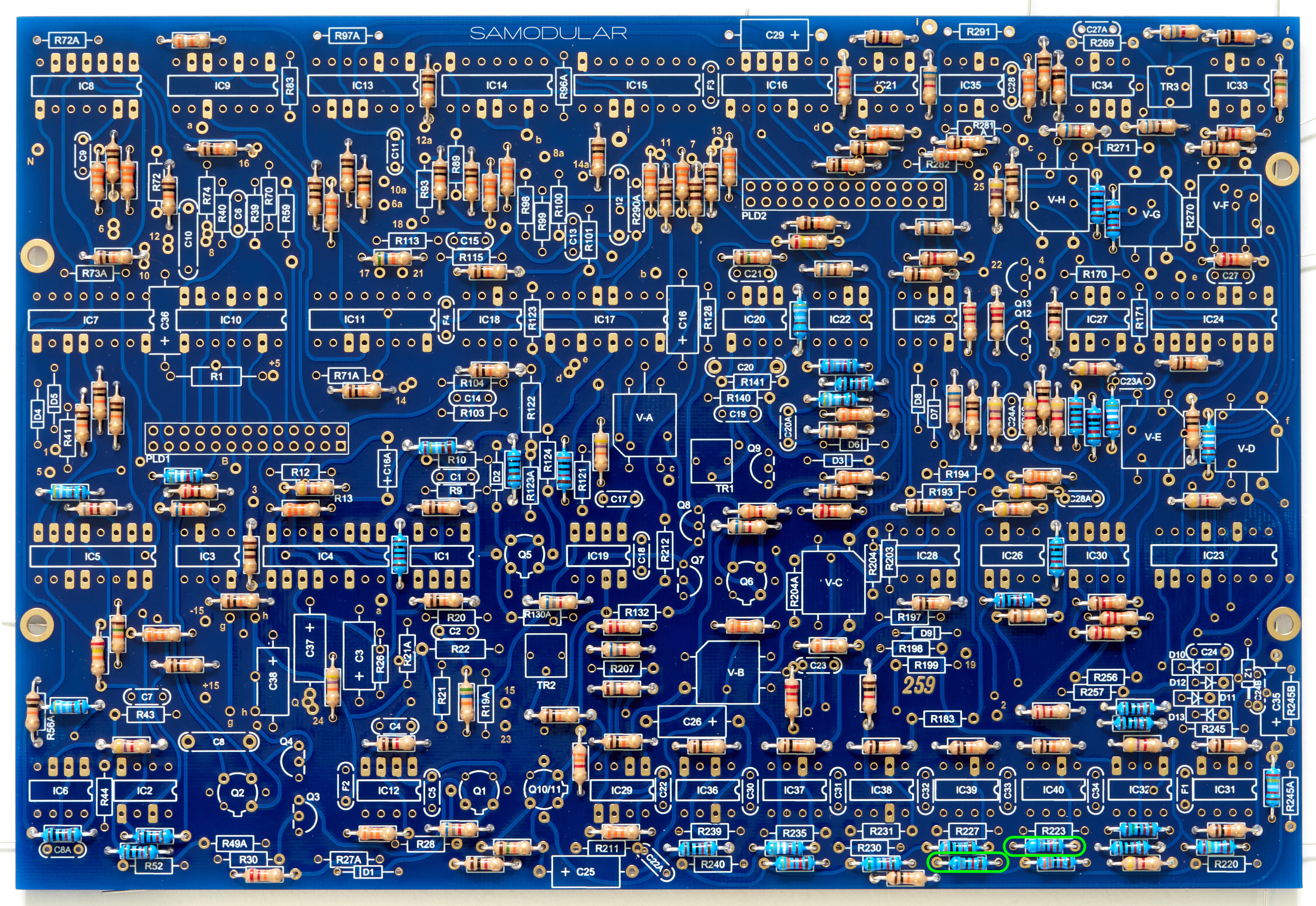
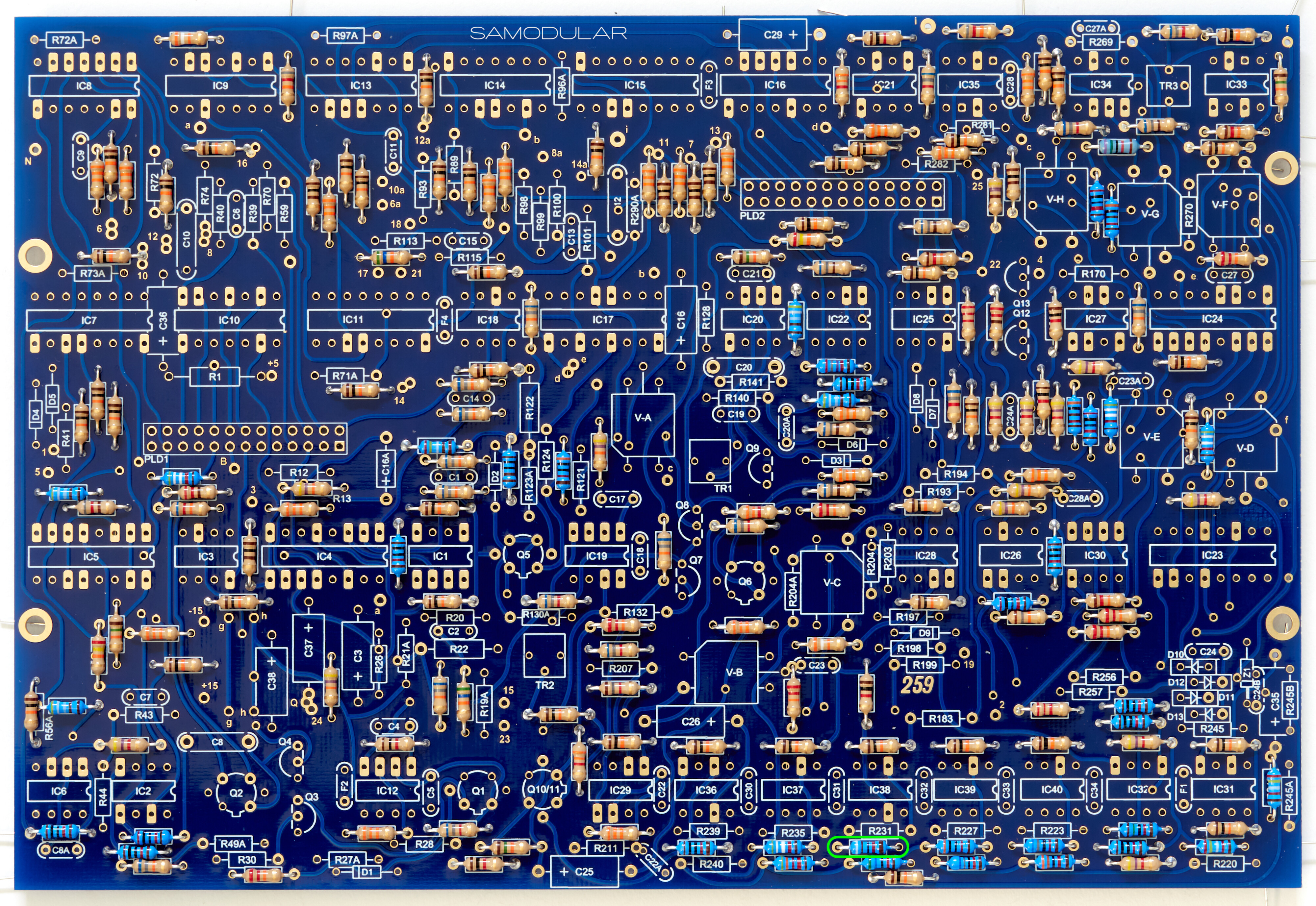
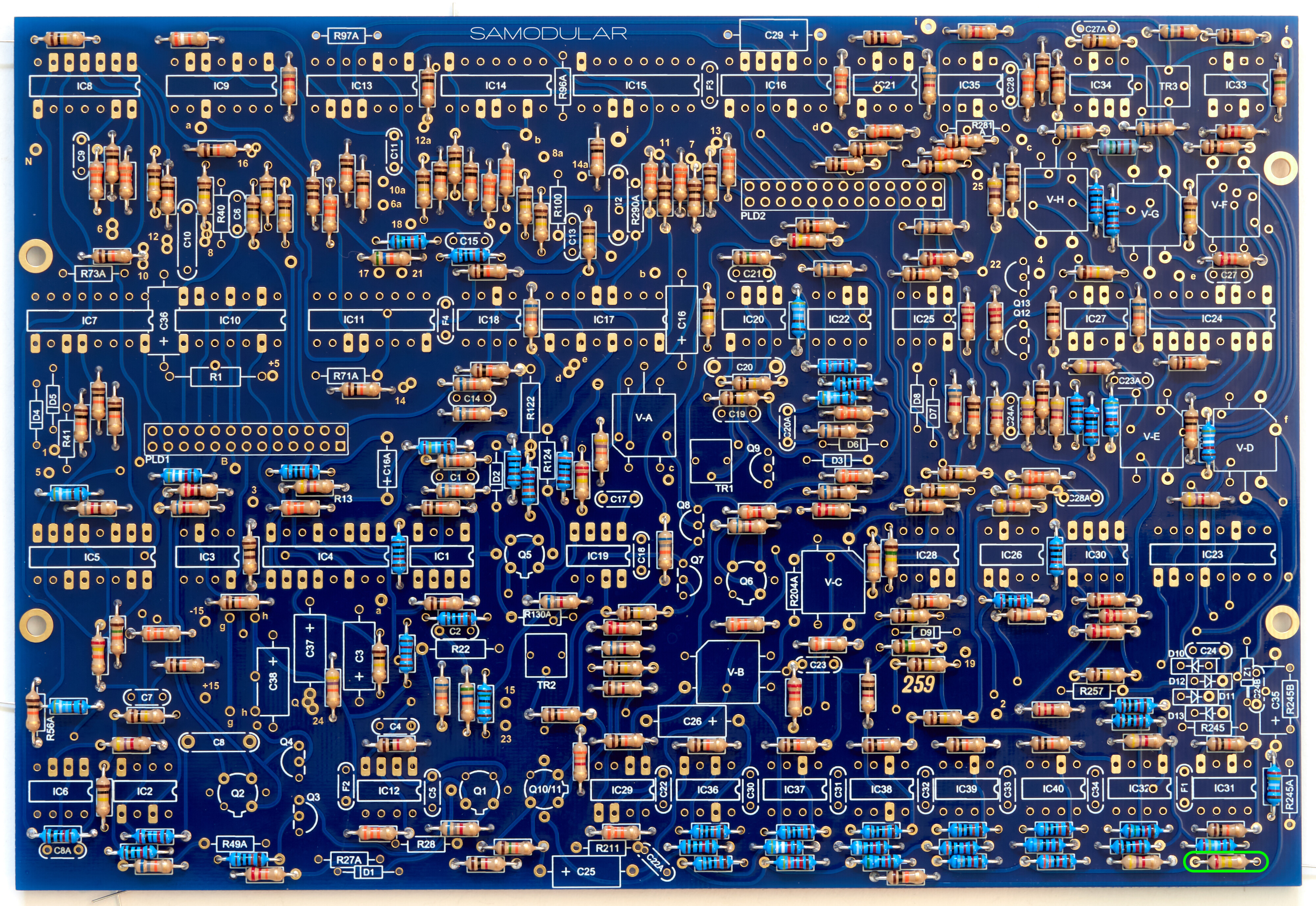
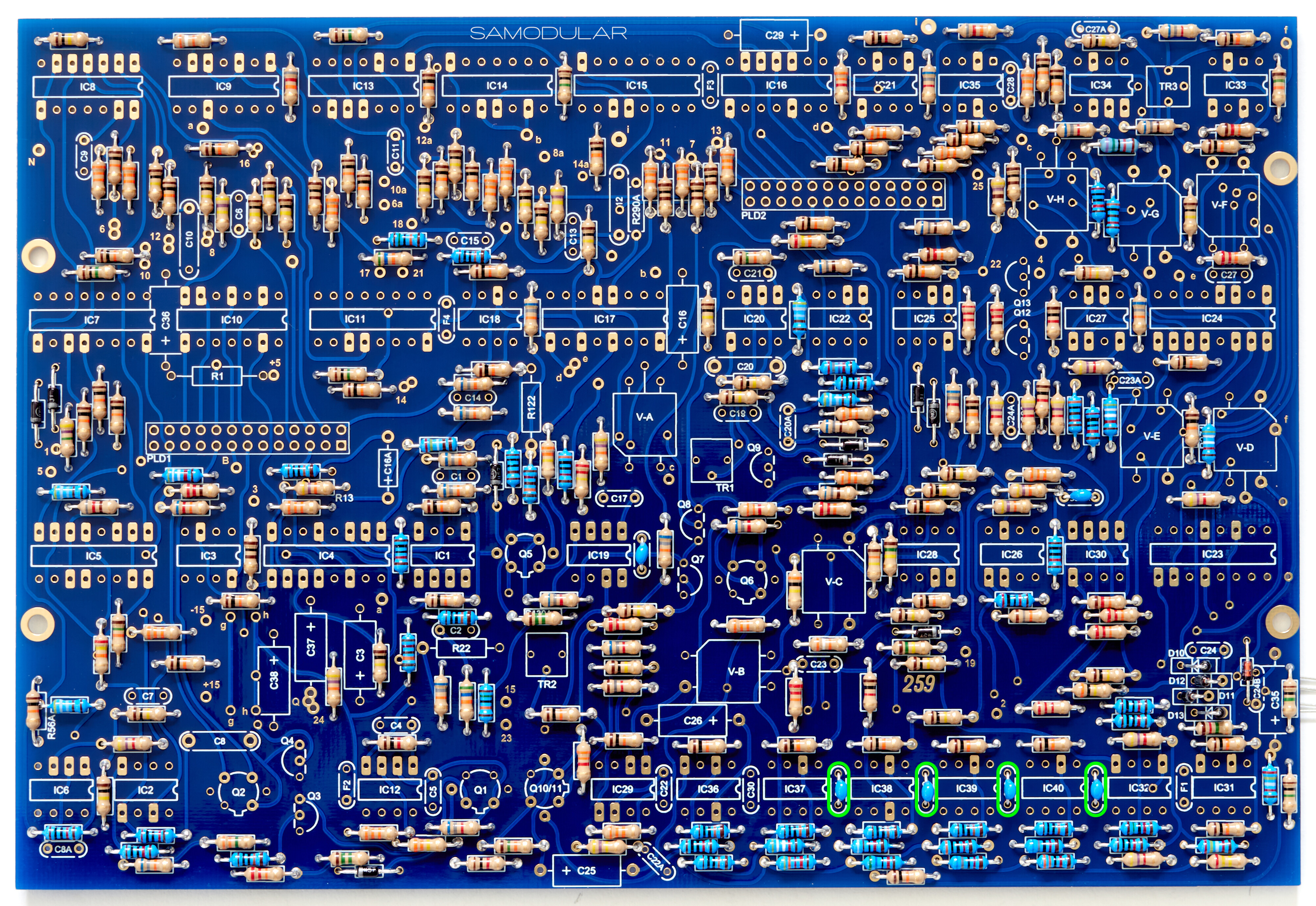
After all diodes and resistors (22R – 10K) have been placed you can start soldering them.
To make sure you do not overheat components. Please only solder one side of a component and then move on to the next component. Once you have finished soldering one side of each component move on with the other side of each component. When you are done your PCBs should look like on the following pictures.
Click on the picture for a high resolution image.
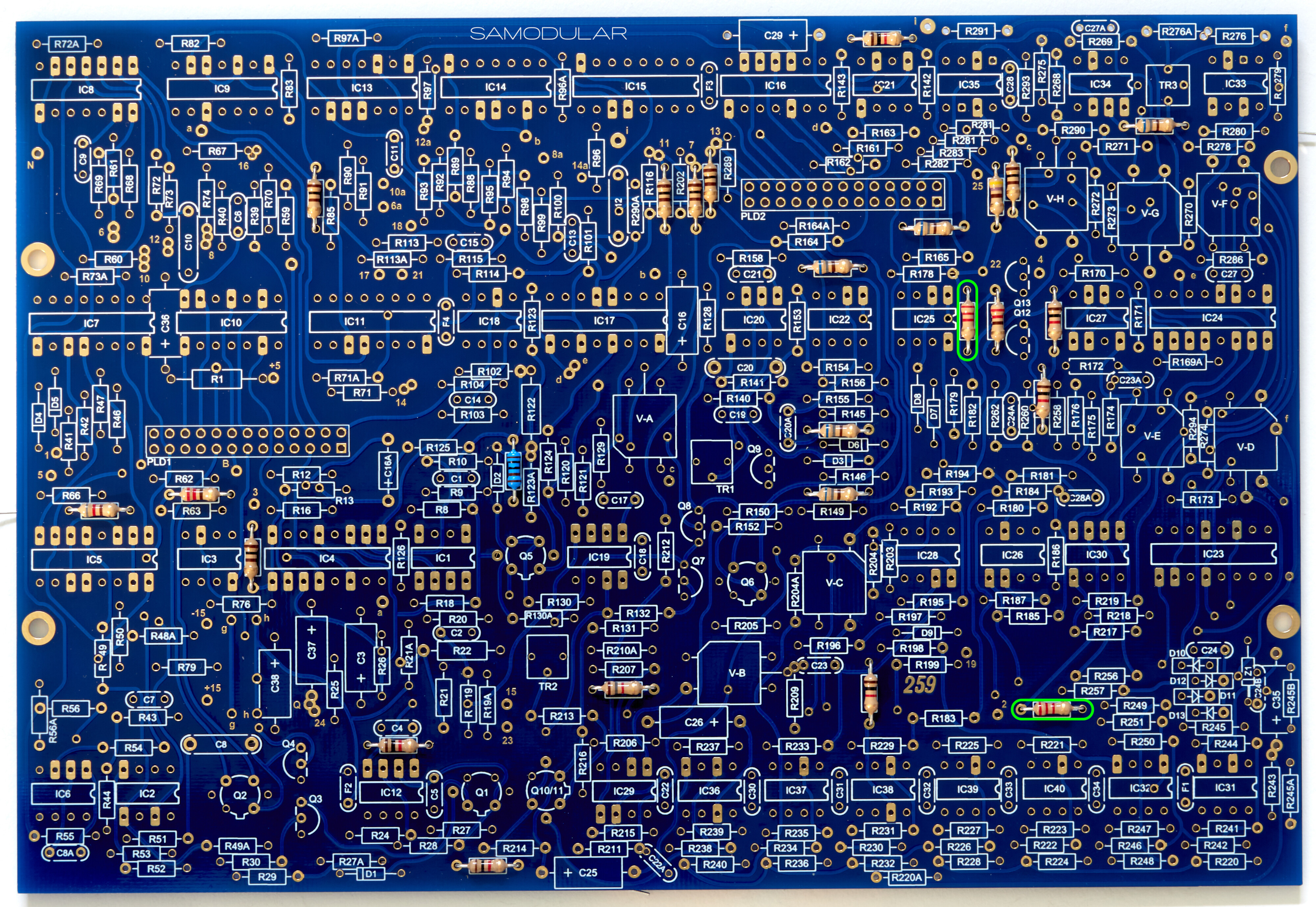
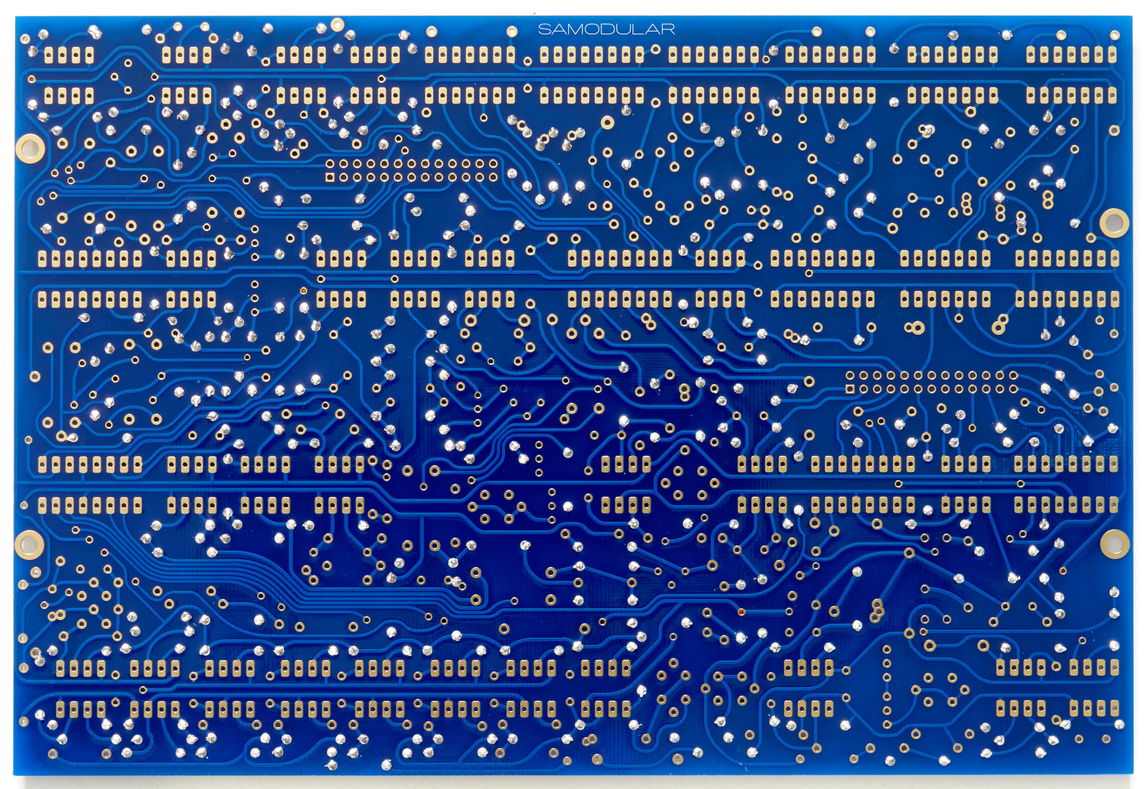
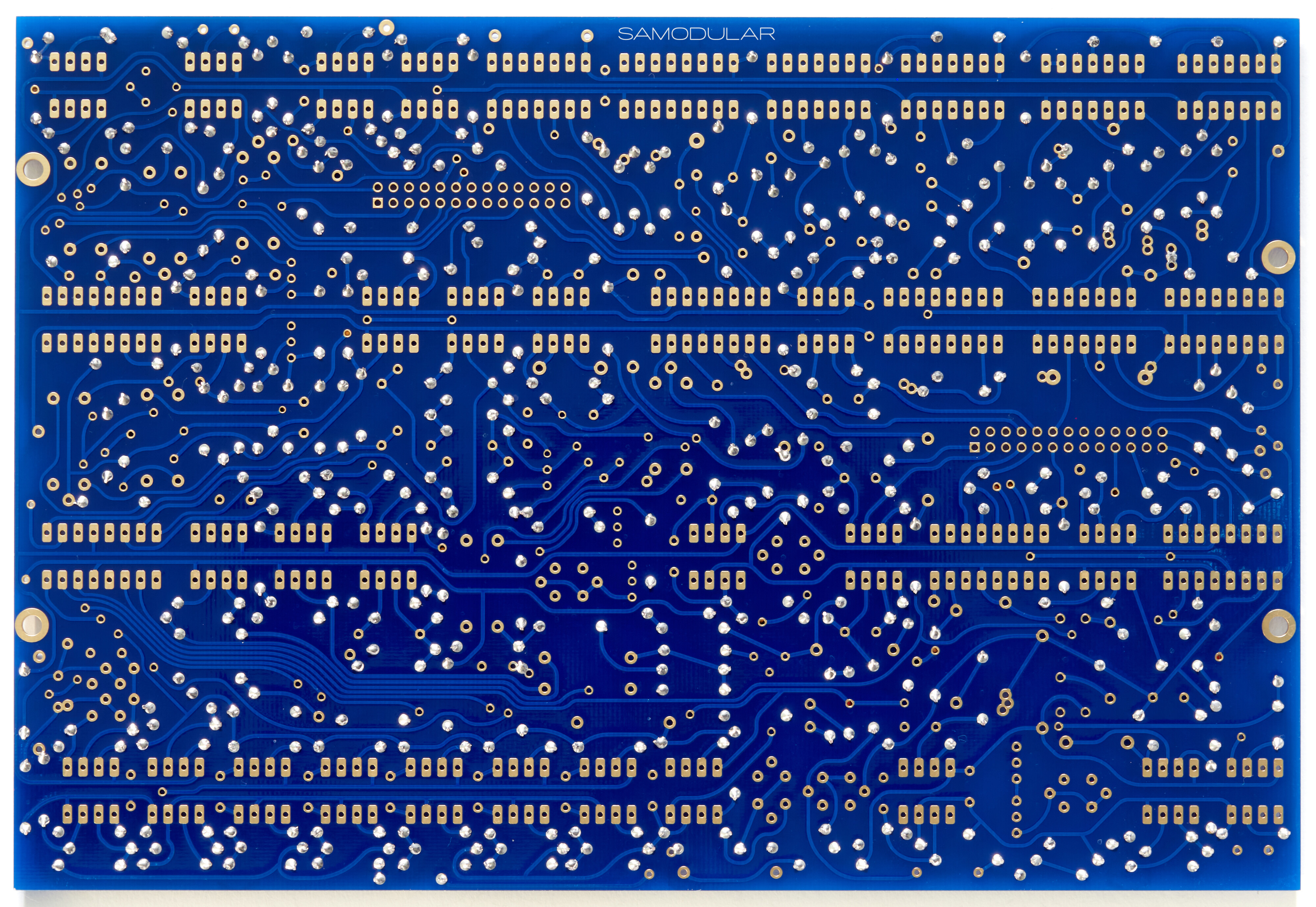
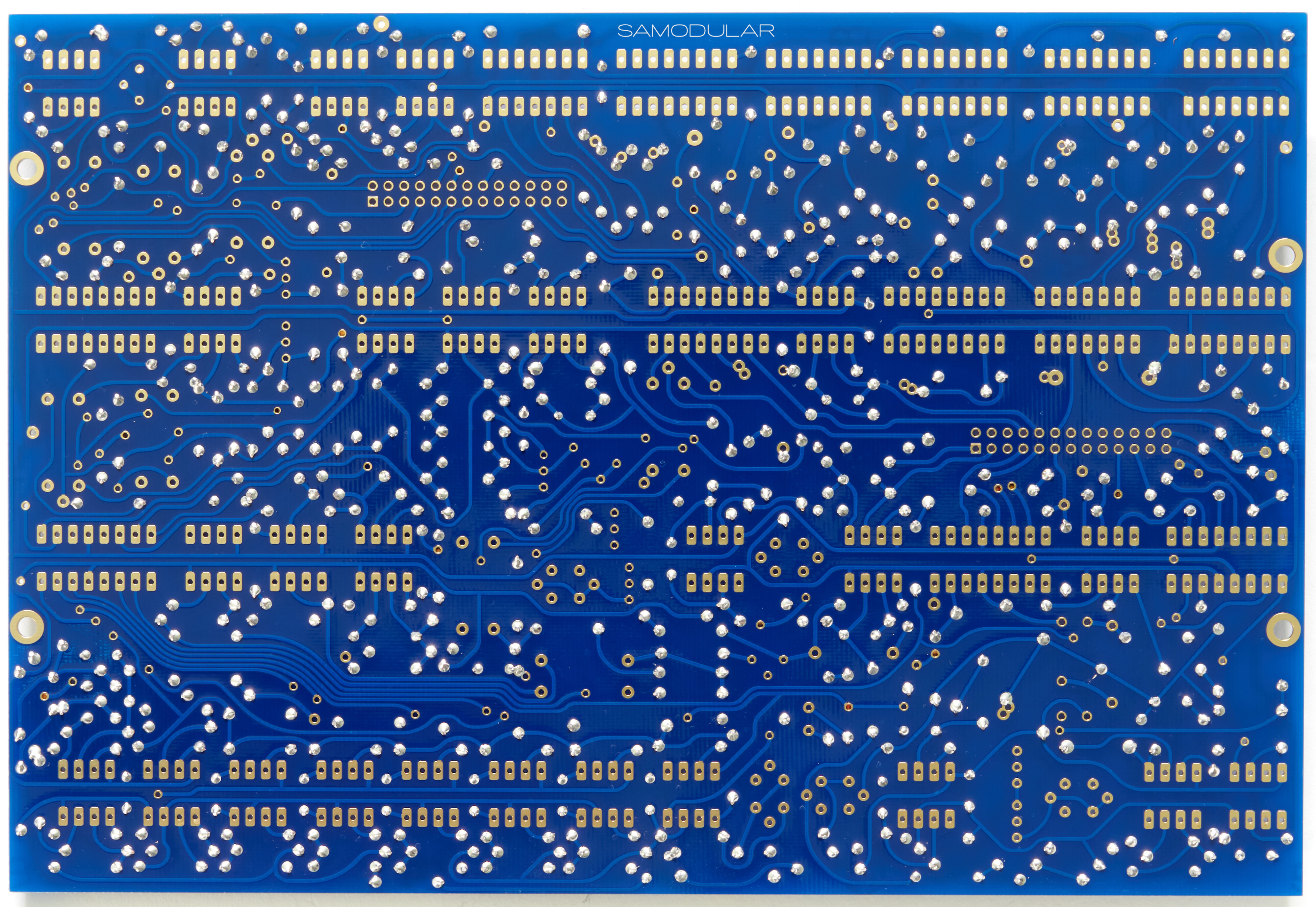
After soldering snip off all component leads.
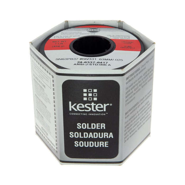
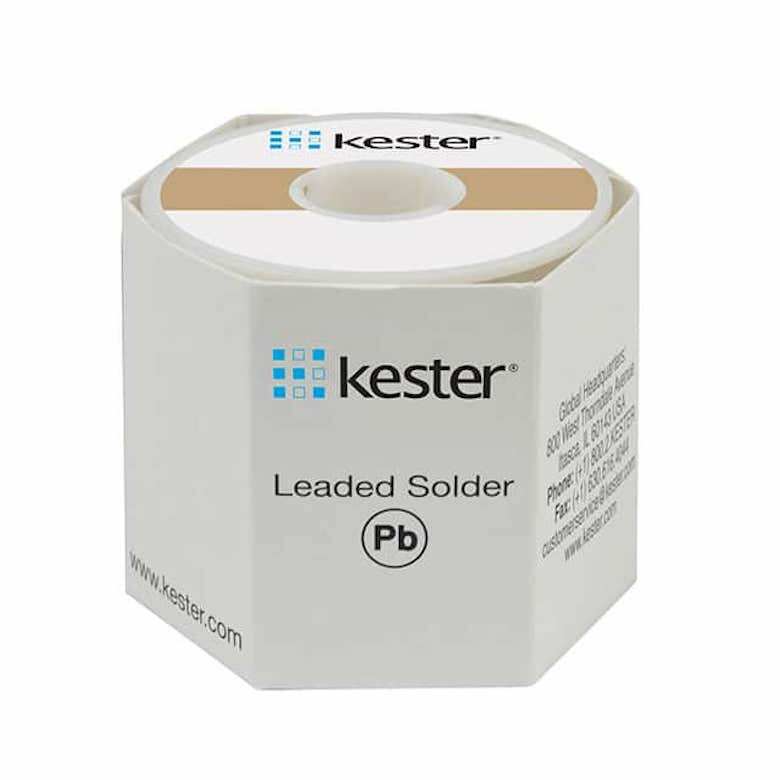
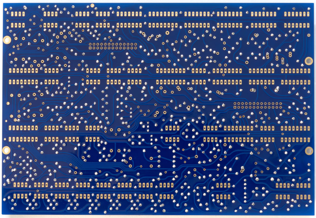
It is important to WASH your soldered PCBs. If you have used my recommended water soluble solder from Kester take your PCBs to your bathroom and wash them thoroughly under water for about 3 minutes. After that please use a hairdryer and thoroughly dry your PCBs. If you have used regular solder please wash with isopropyl alcohol or flux cleaner. From my experience I get the best looking results with water soluble solder. Once you are done your PCBs should look like this:

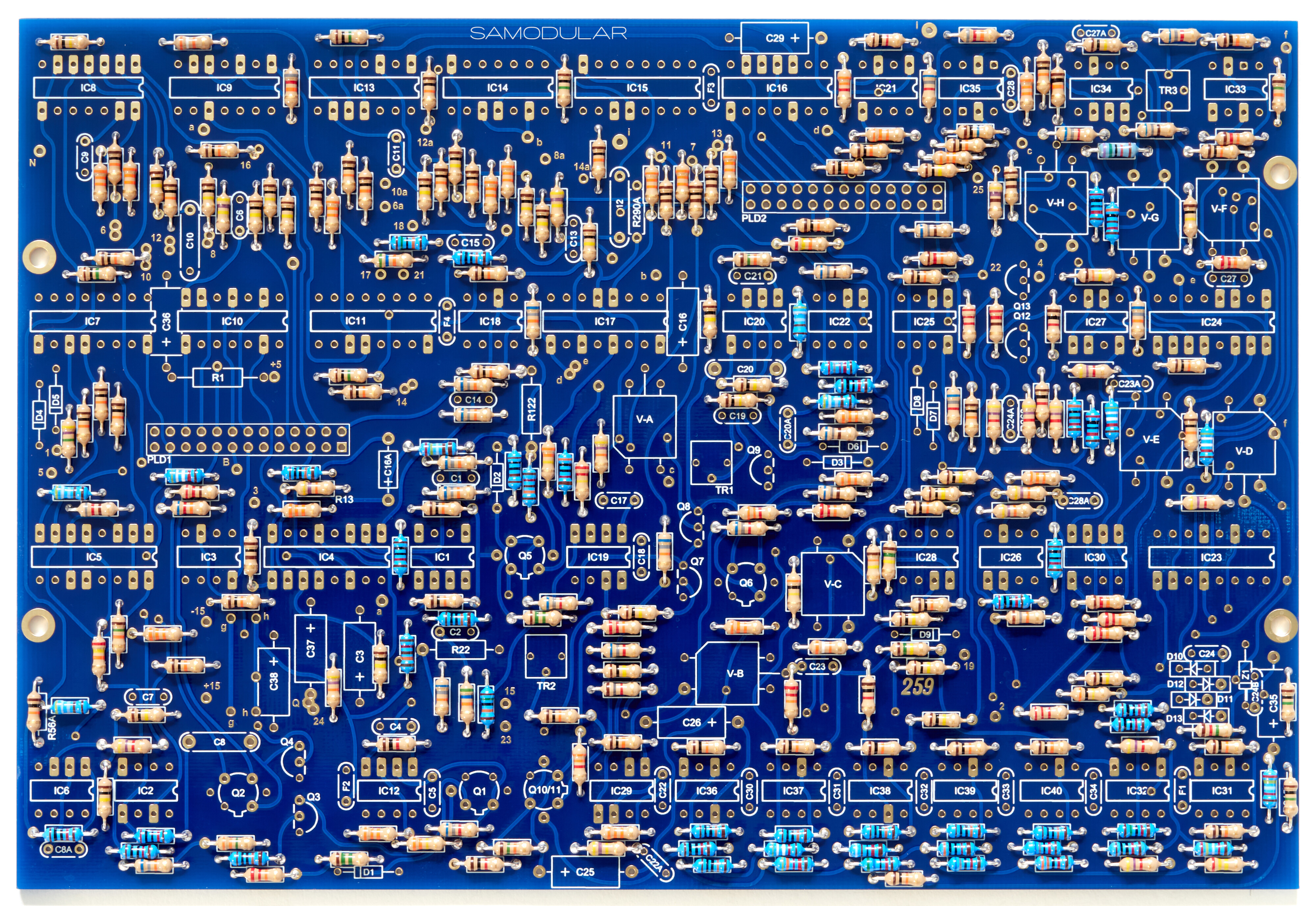
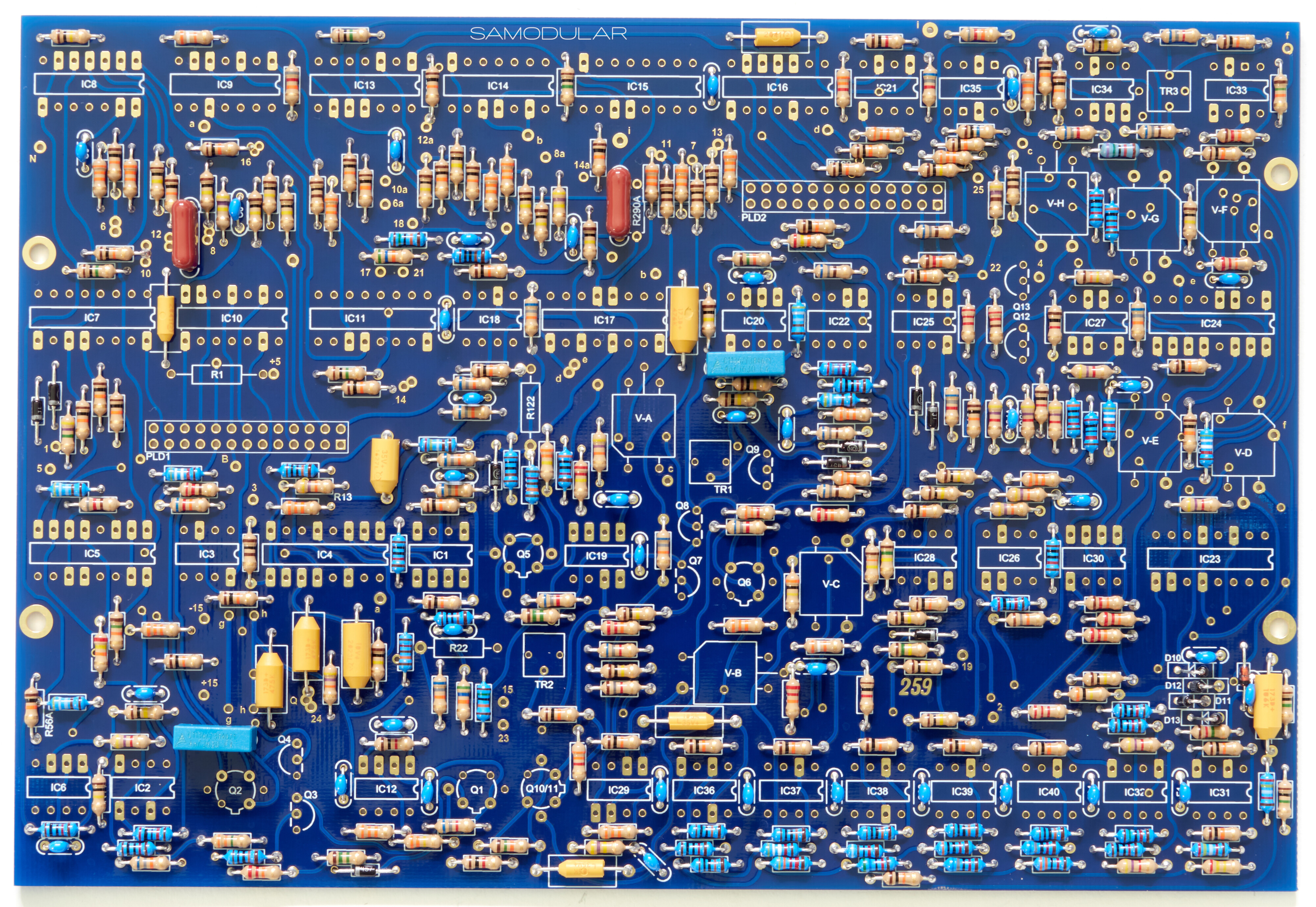
Part 2 – PCB2
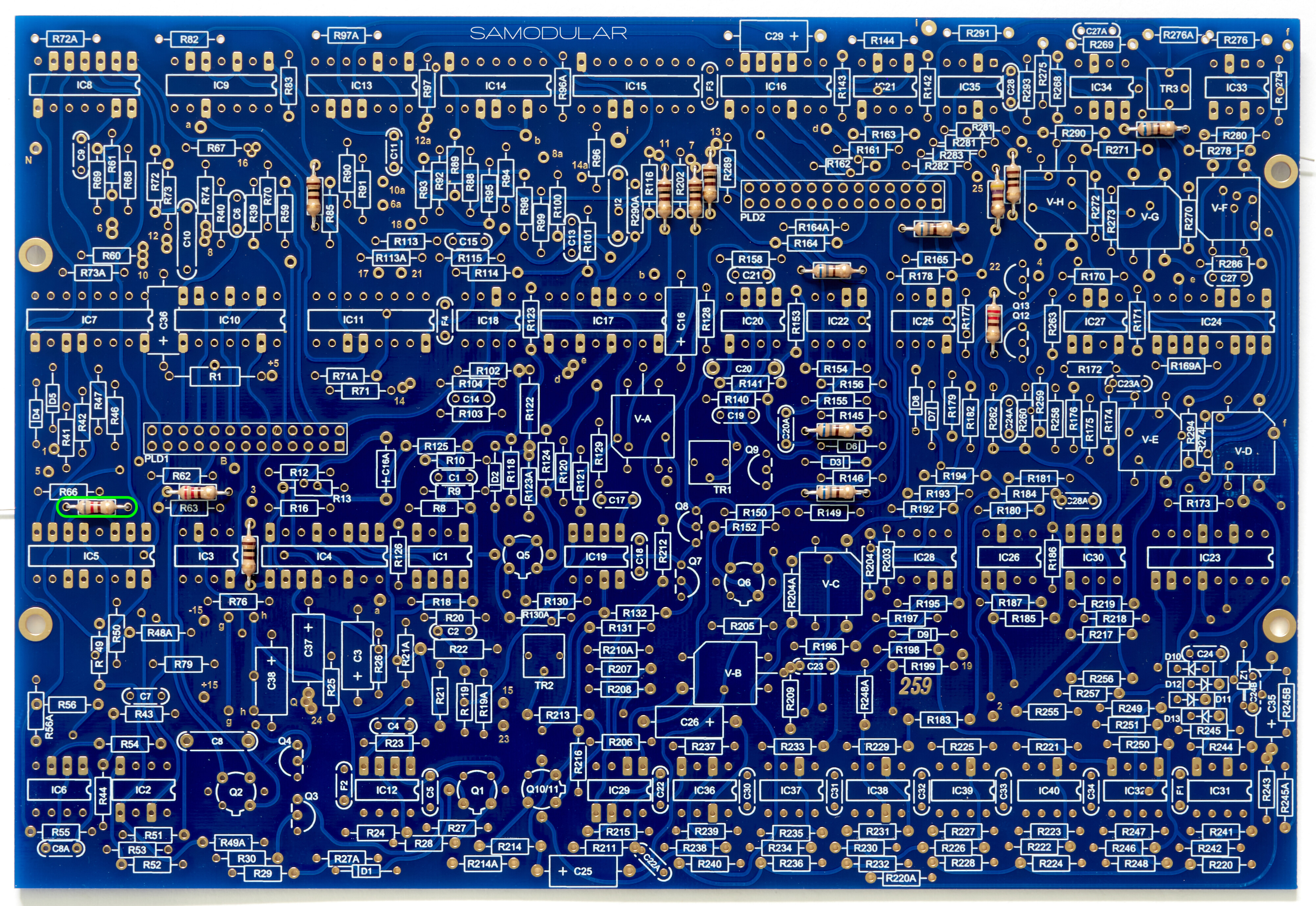
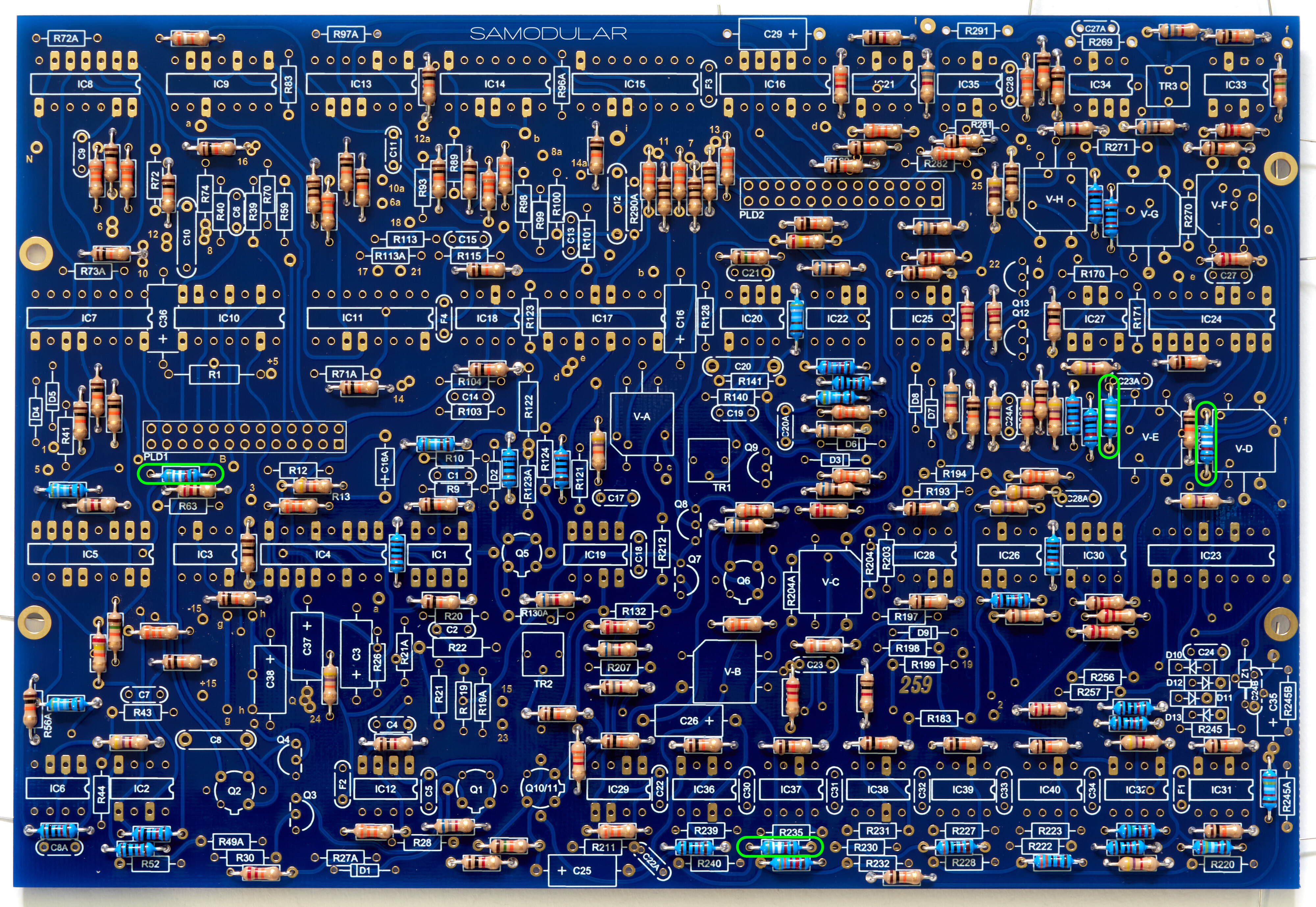
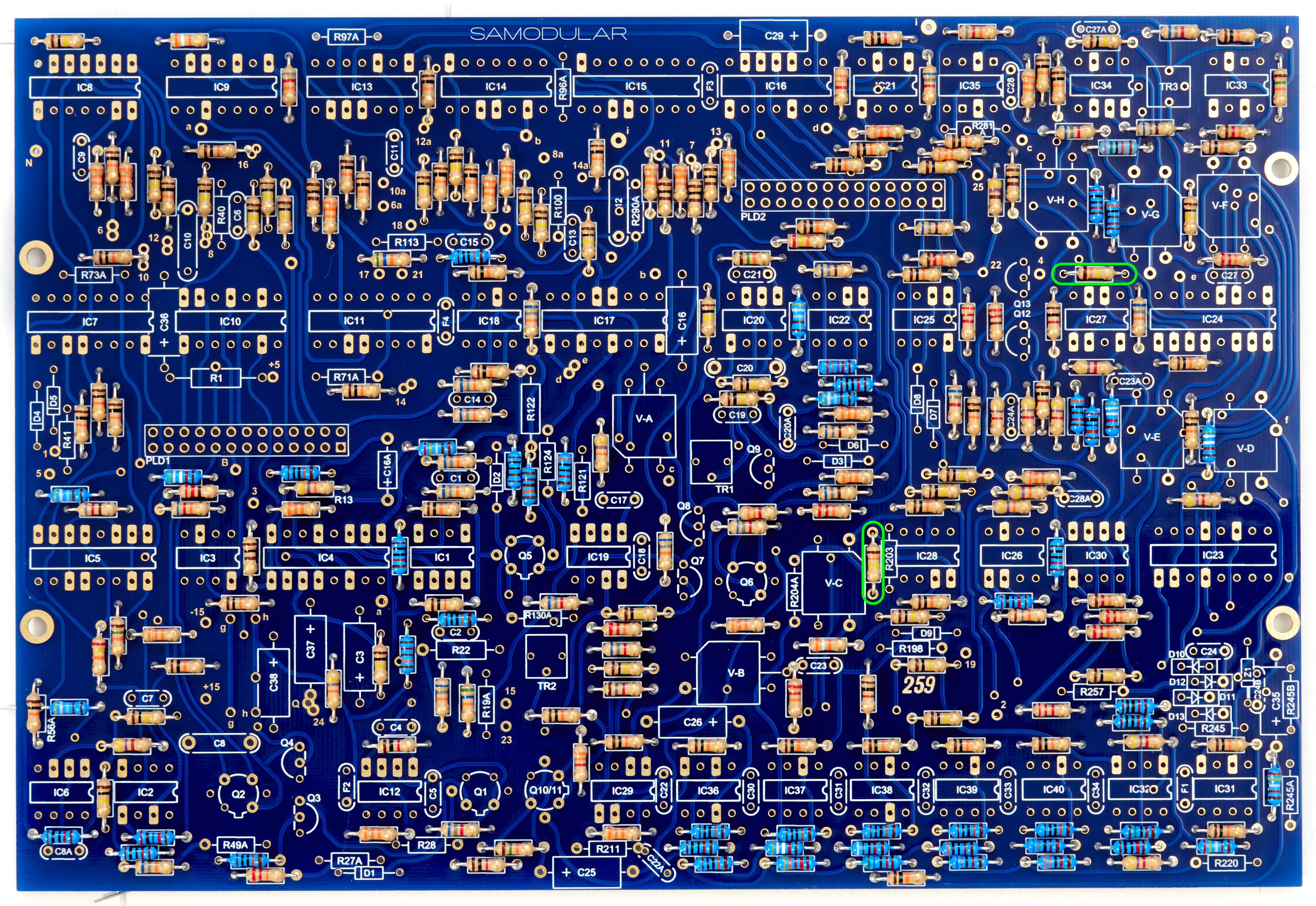
Placing resistors (12K – 91K)
Repeat the procedure from Part1 – now with 12K to 100K resistors.
Click on the thumbnails below for high resolution images.
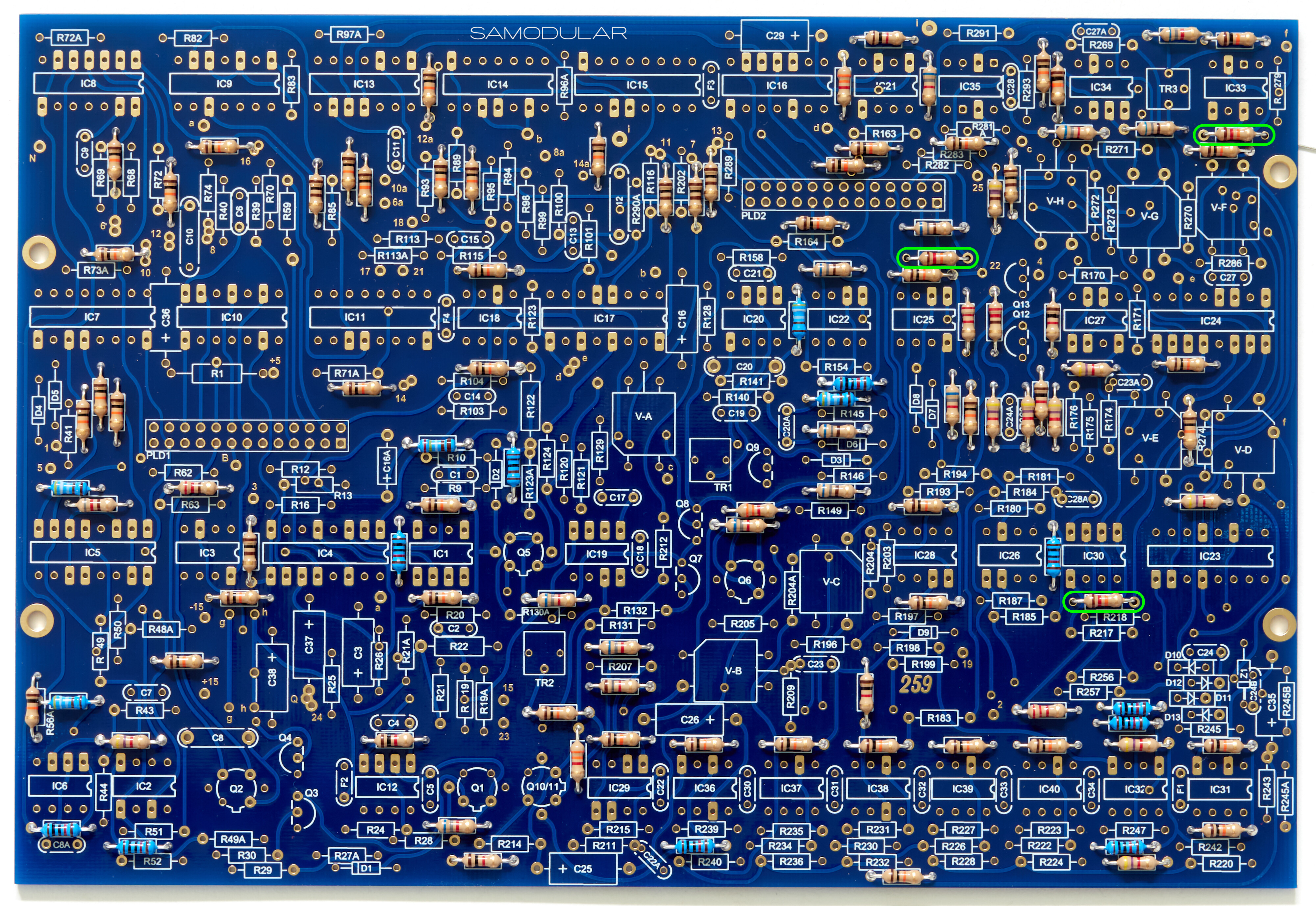
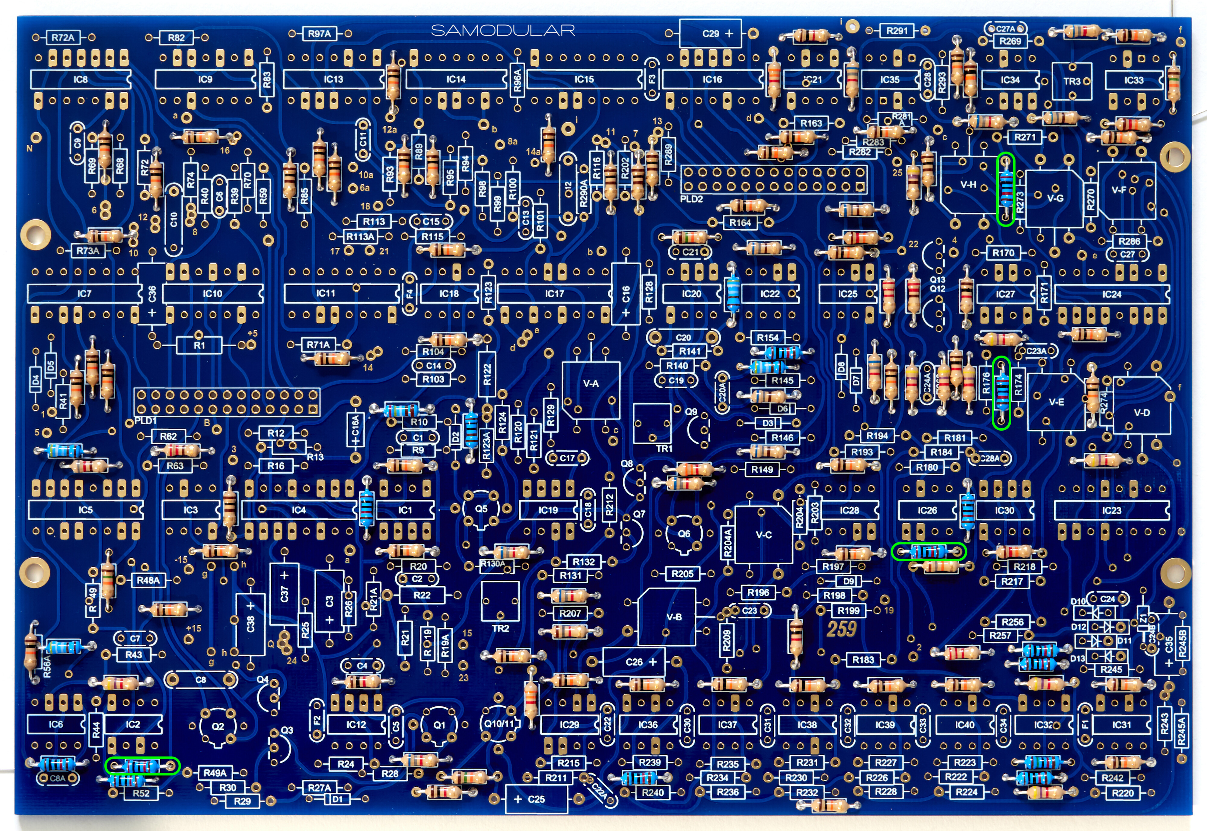

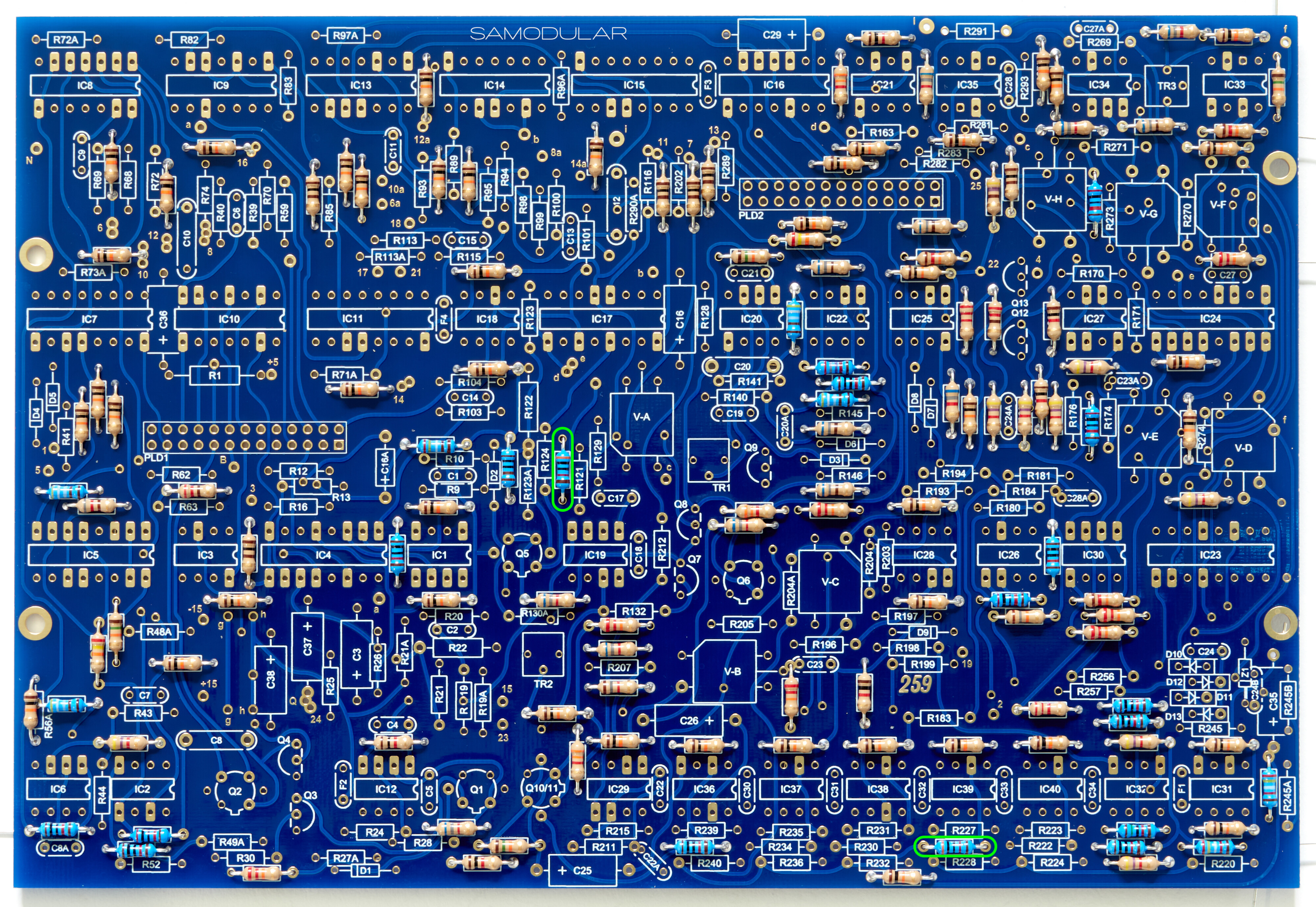


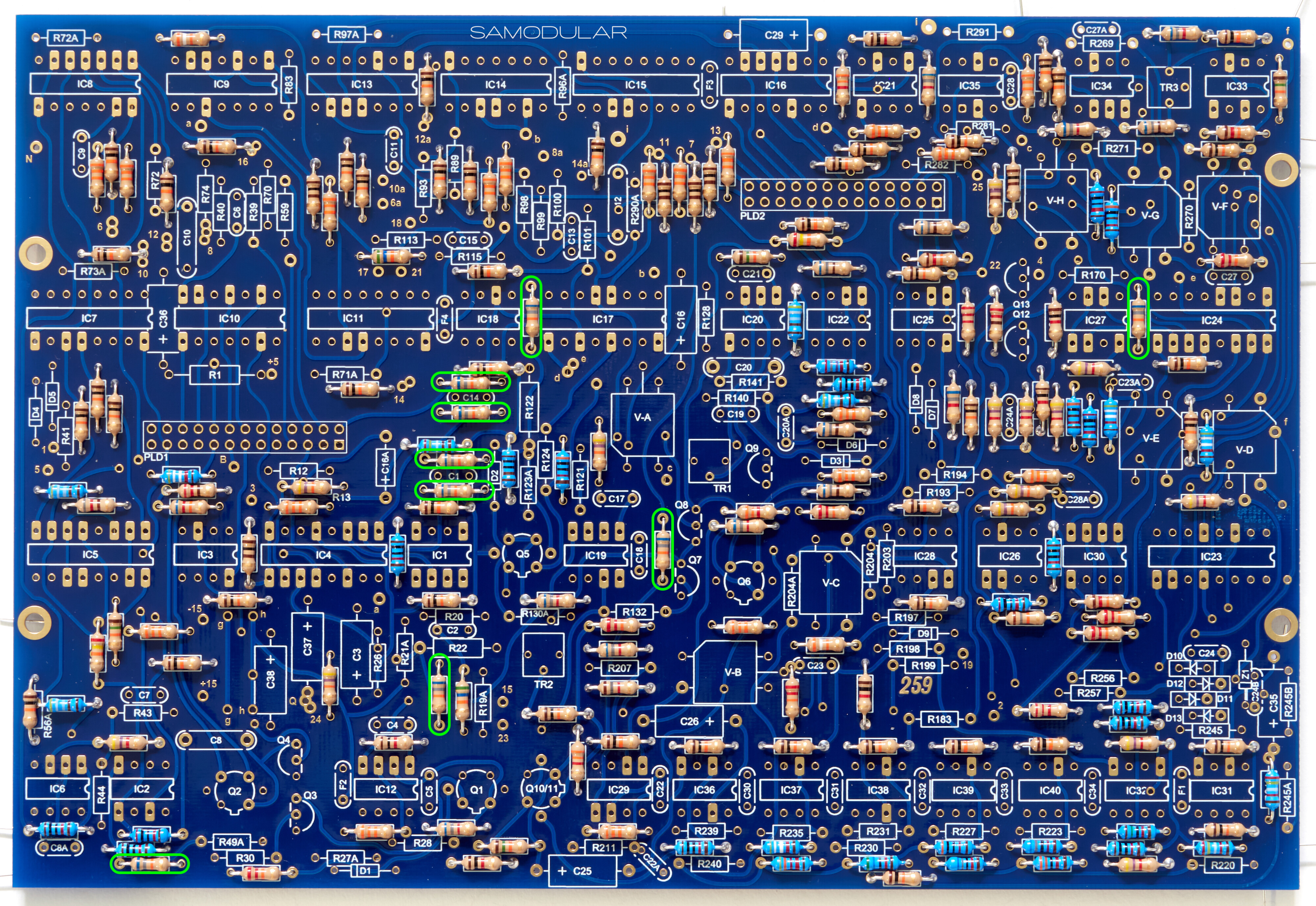

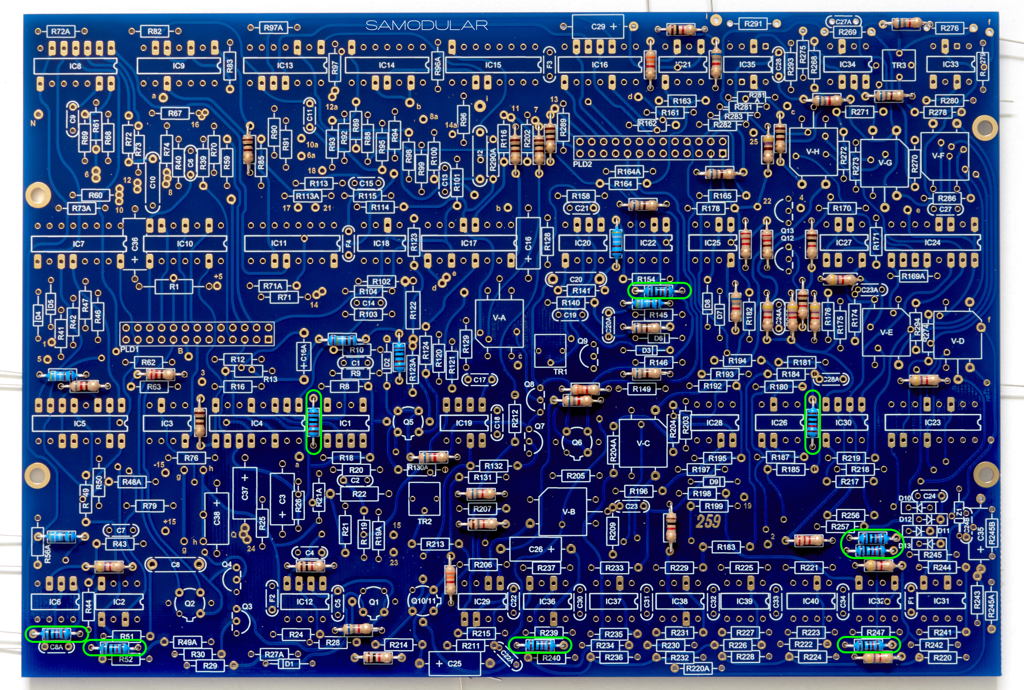
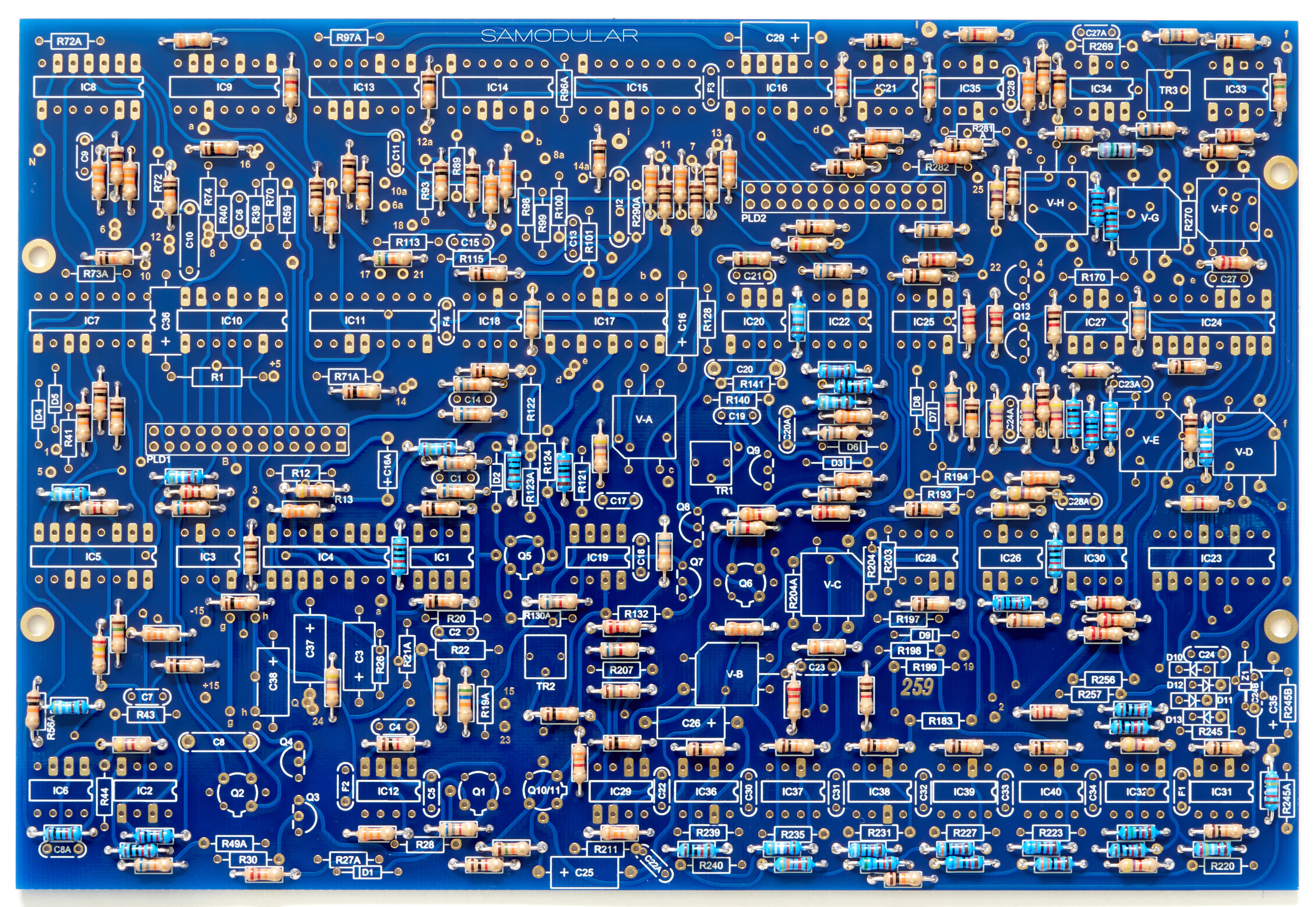
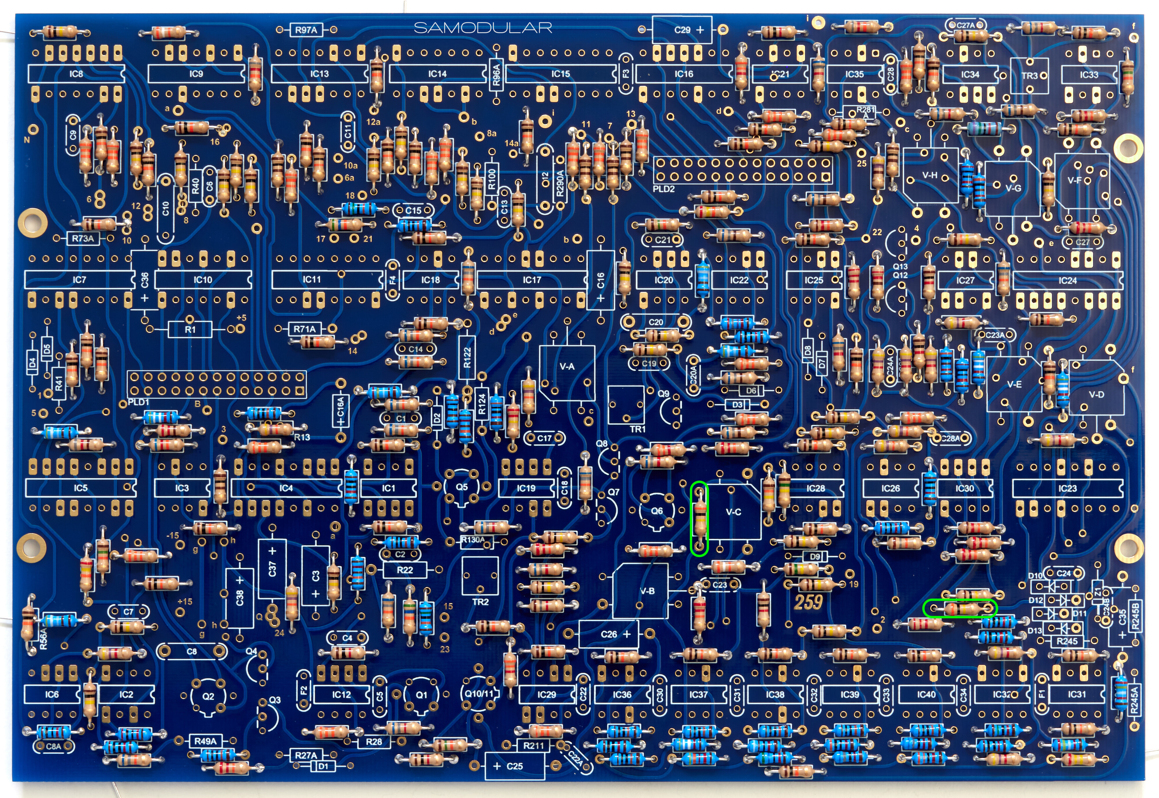
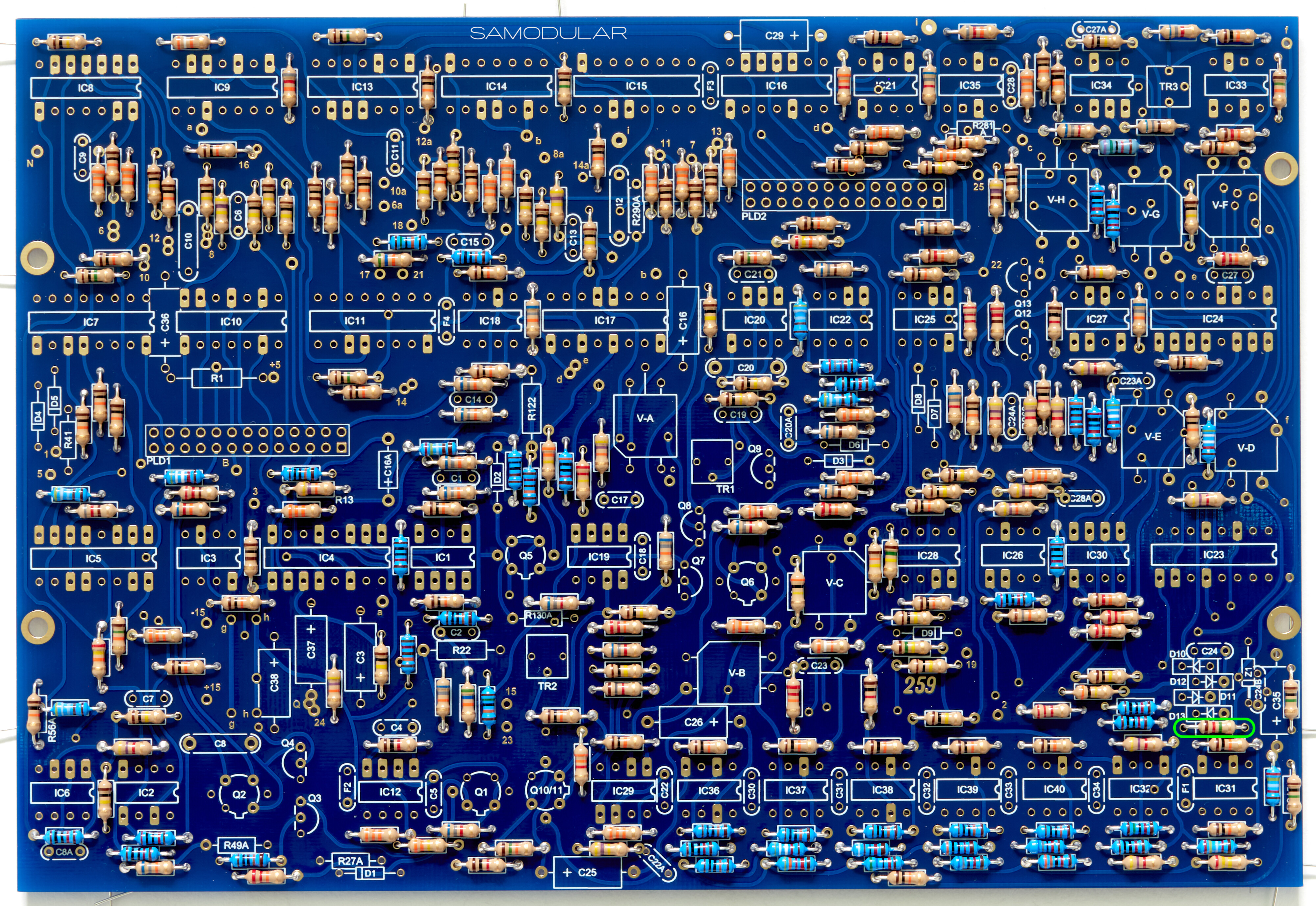
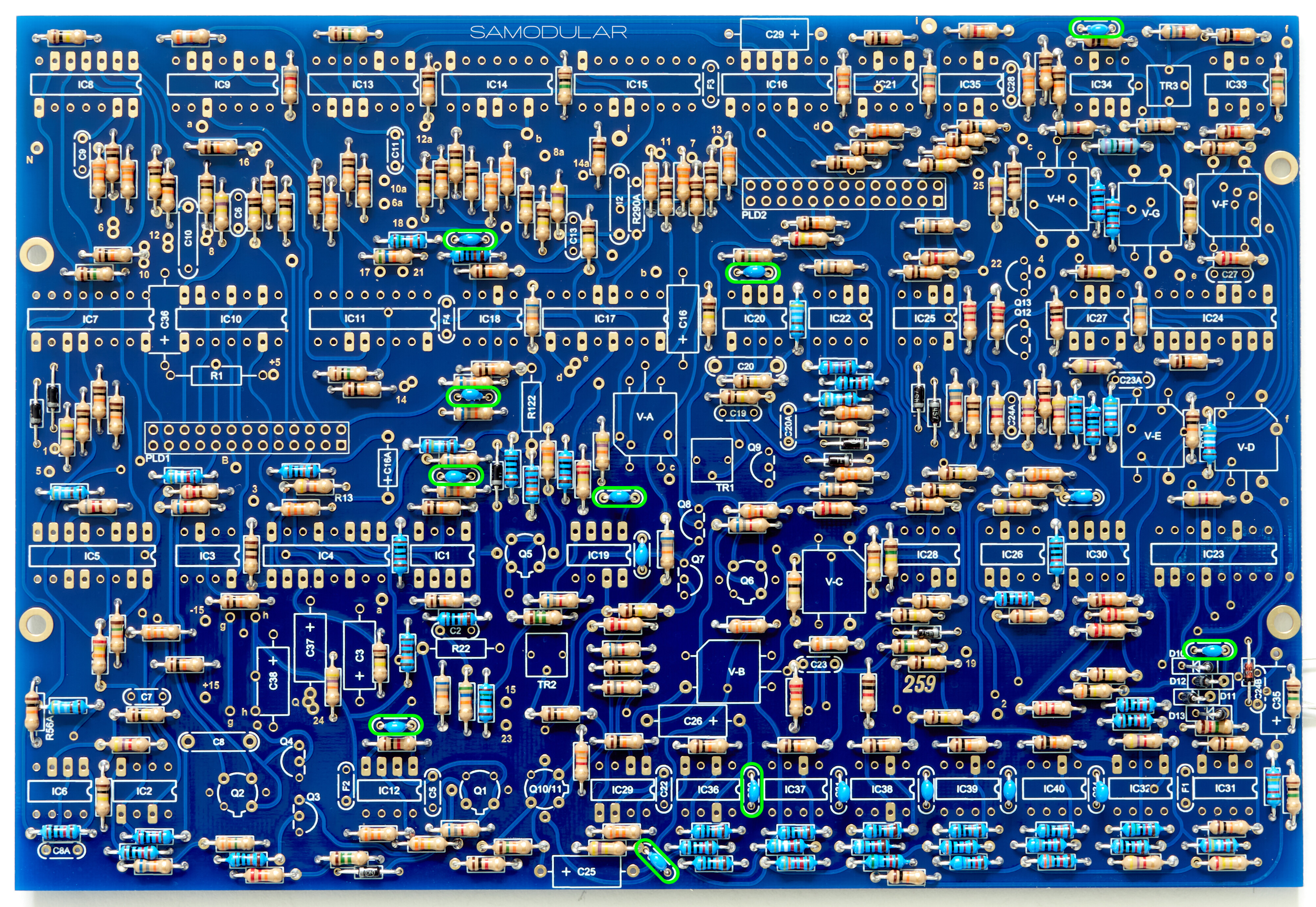
After resistors (12K – 91K) are in place please solder them.
Again – to make sure you do not overheat components. Please only solder one side of a component and then move on to the next component. Once you have finished soldering one side of each component move on with the other side of each component. When you are done your PCBs should look like on the following pictures.
Click on the picture for a high resolution image.

After soldering snip off all component leads.
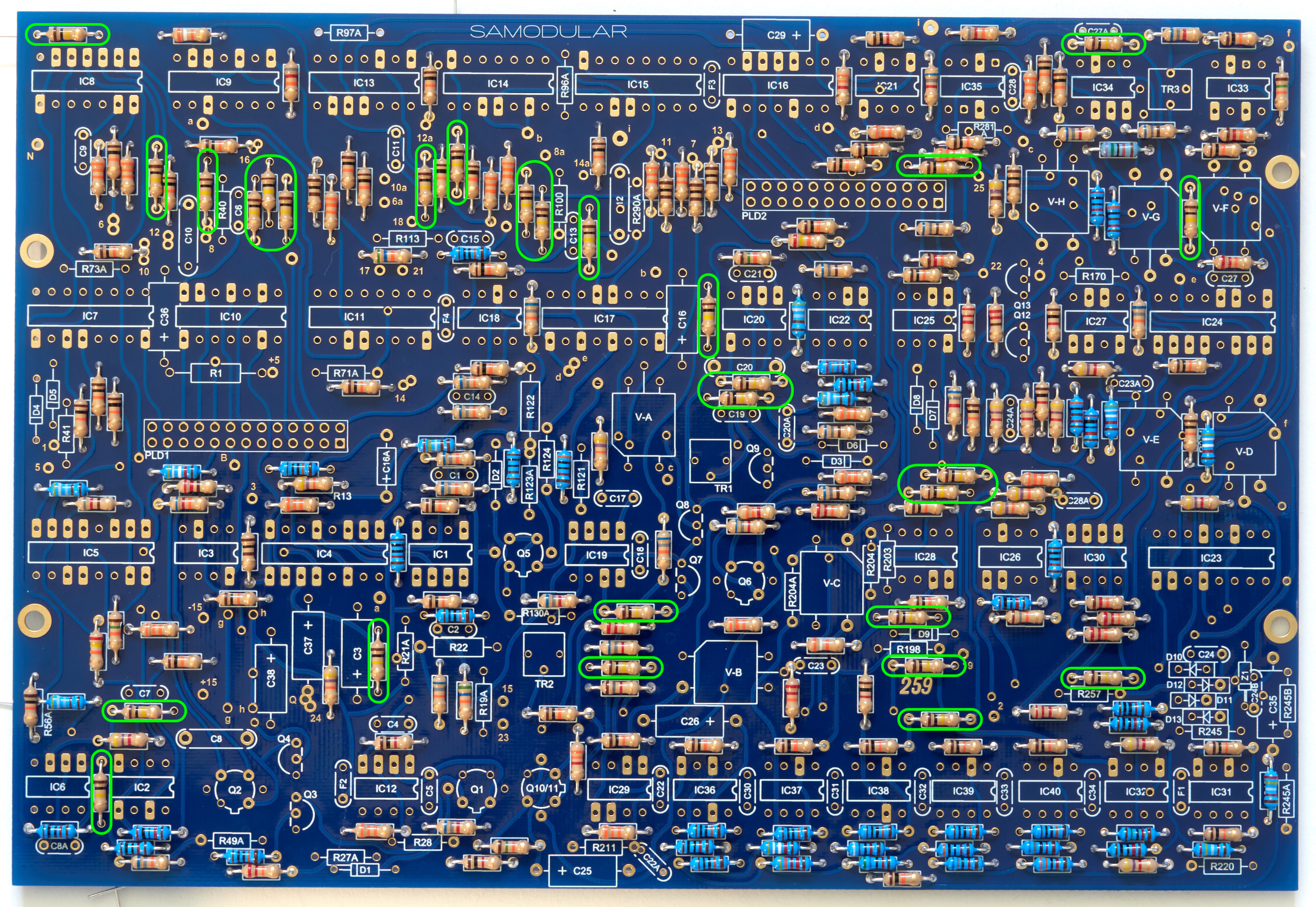
Please wash your PCBs again or if you have plenty of time – move on with Part 3 and wash afterwards. Just make sure you don’t put the PCBs away for a few days with solder flux on the boards if you cannot proceed. Once you are done your PCBs should look like this:
Click on the pictures for high resolution images.
Part 3 – PCB2
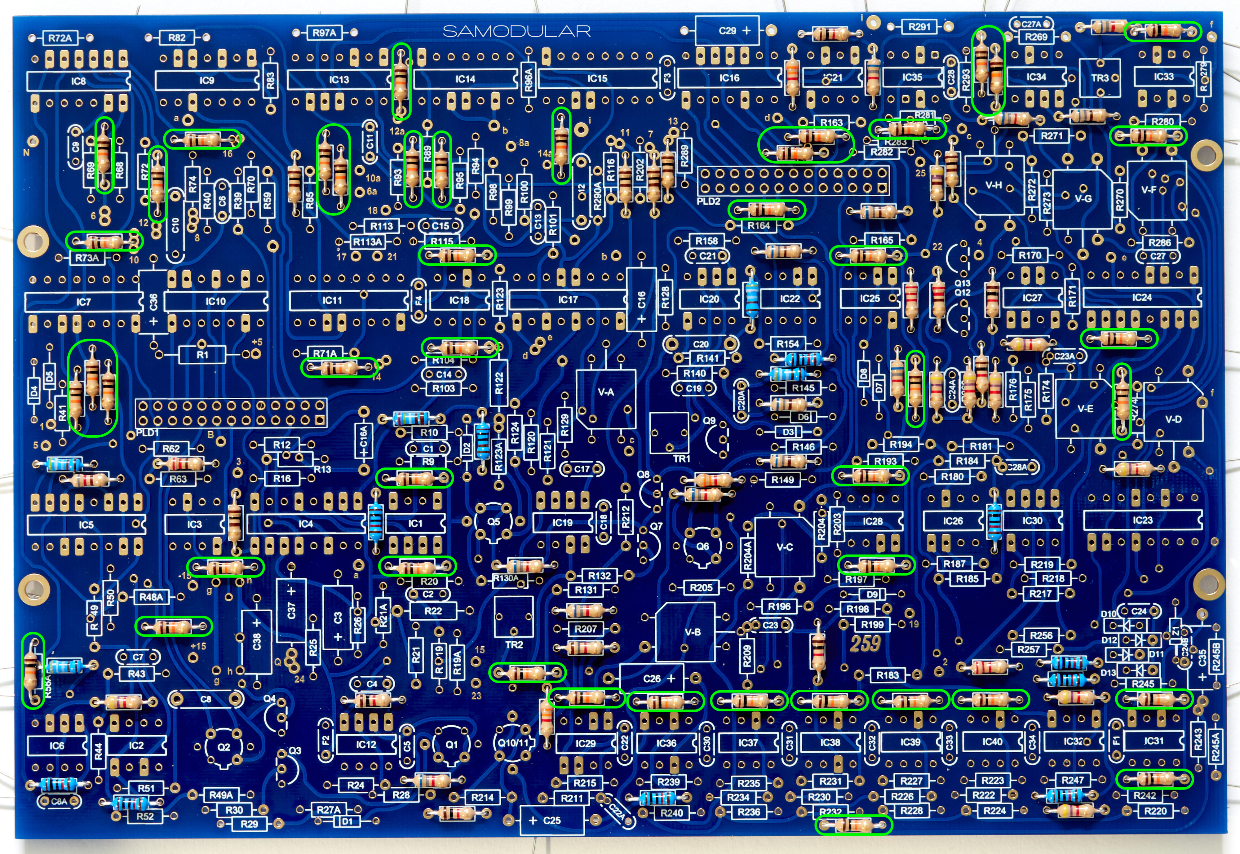
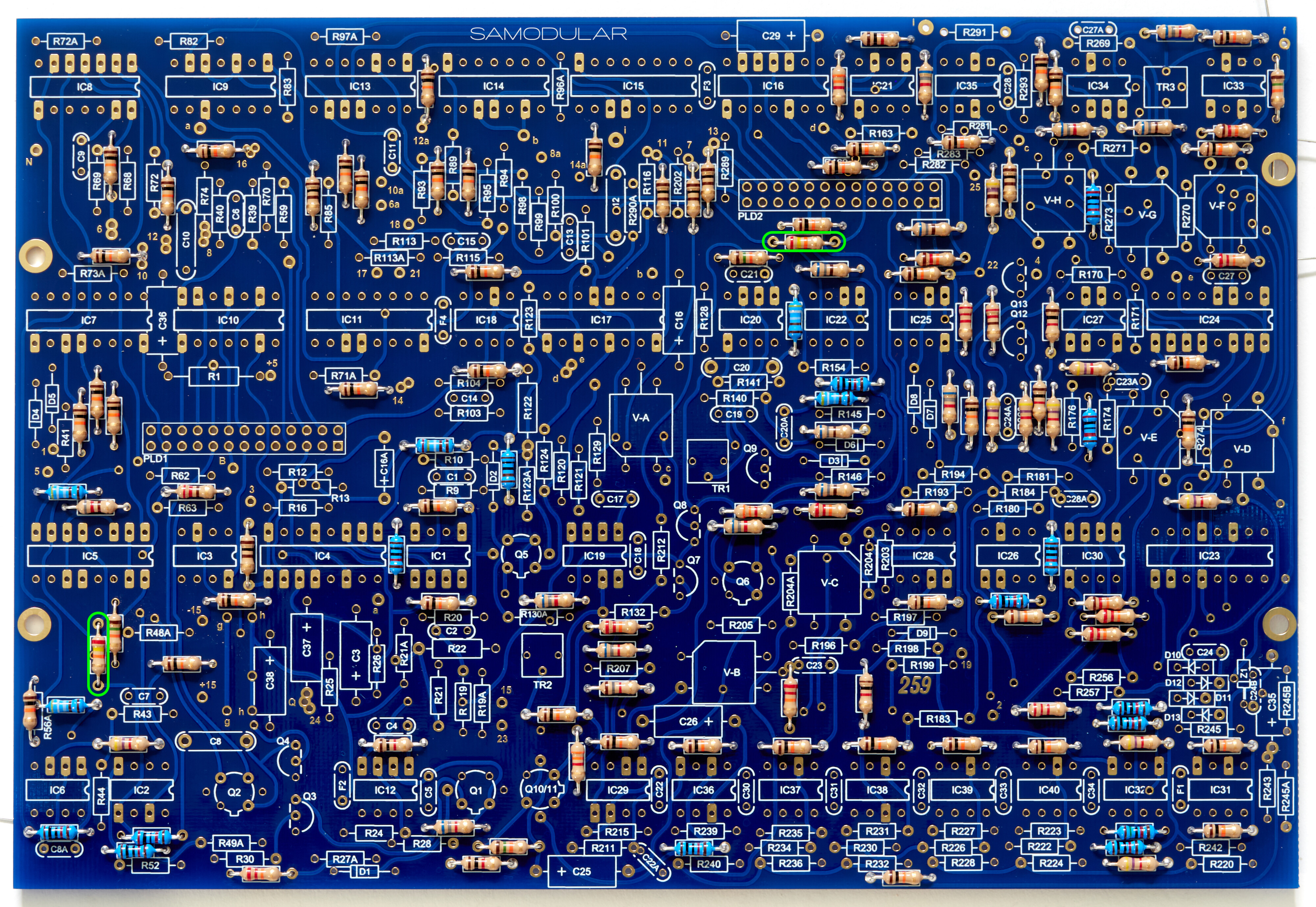
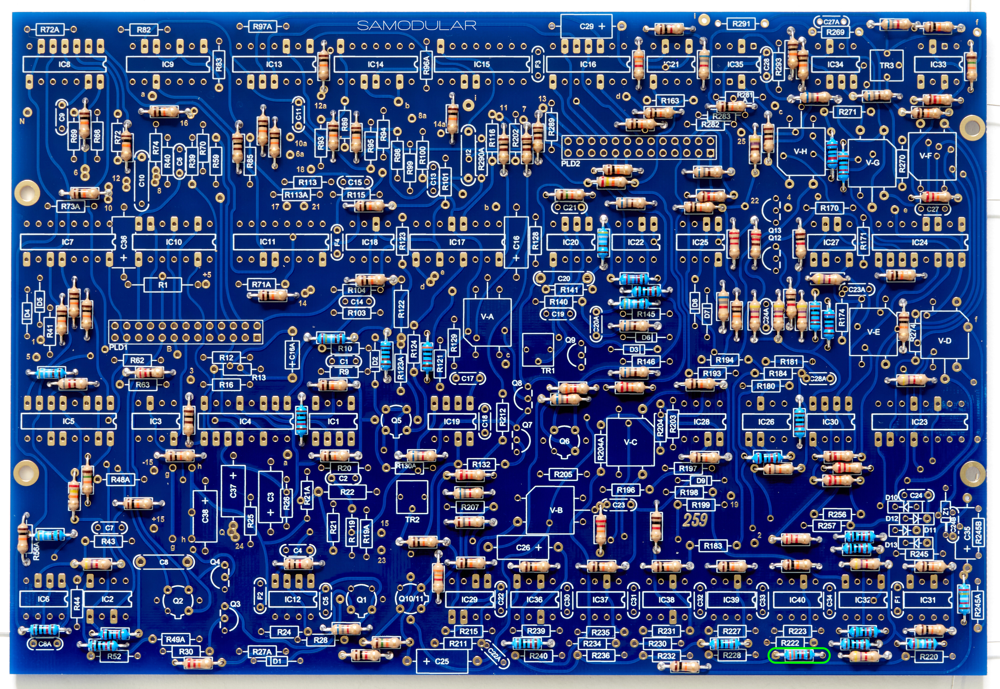
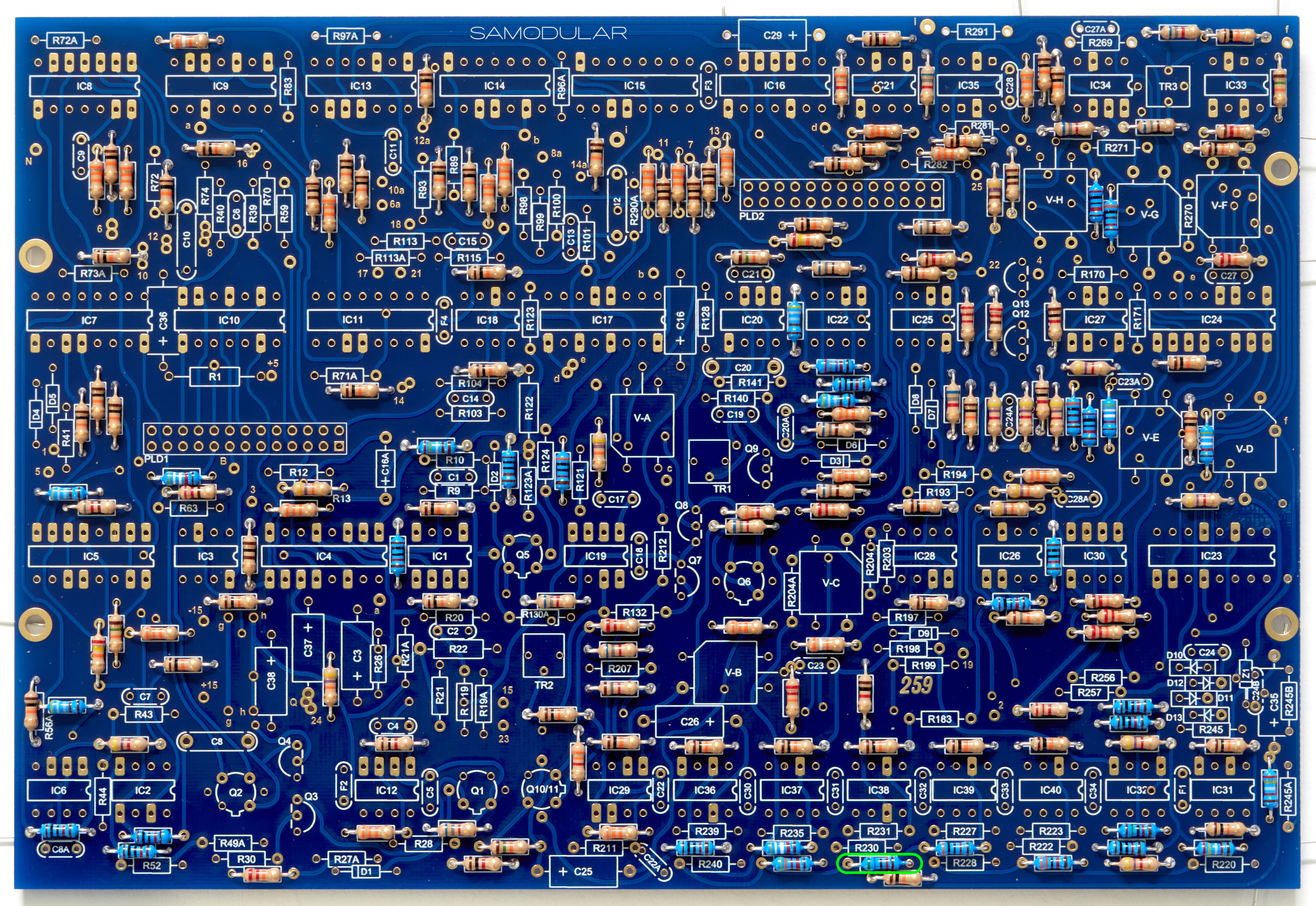
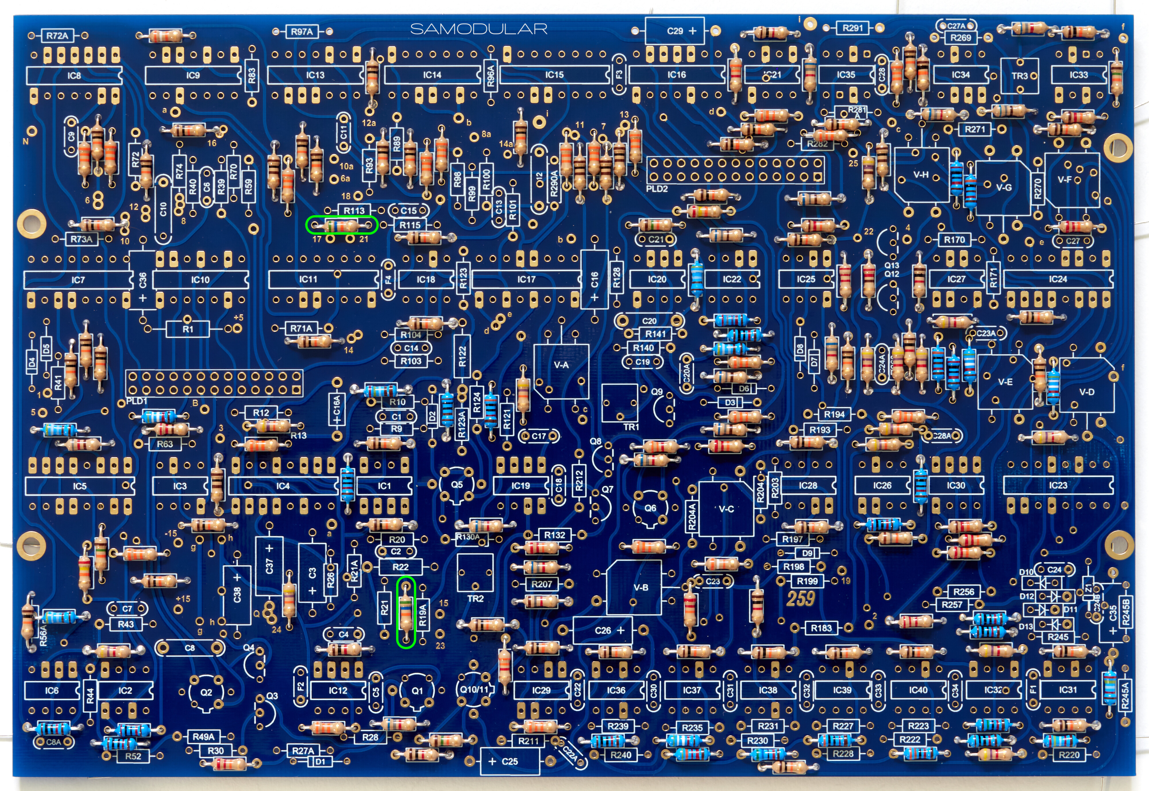
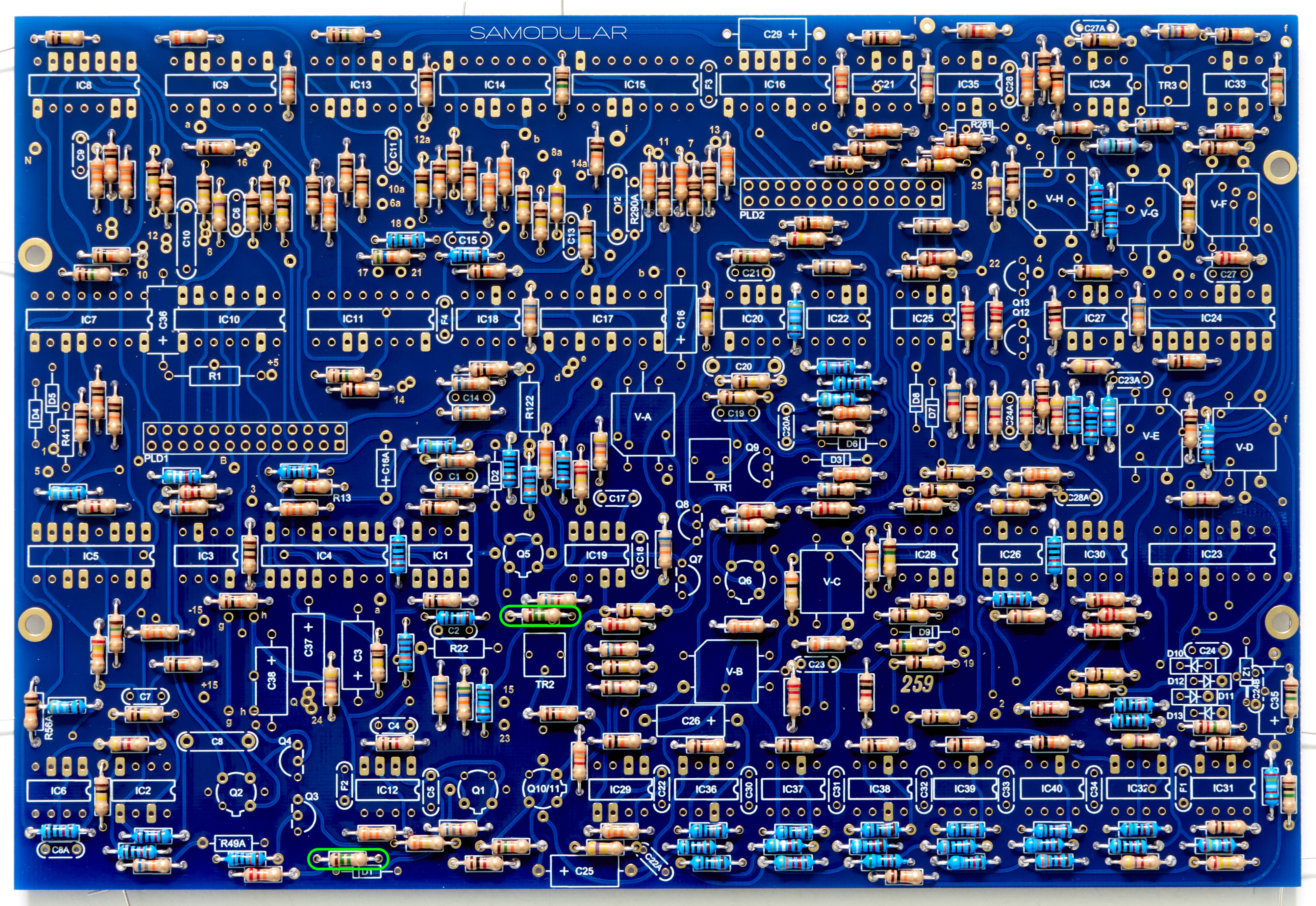
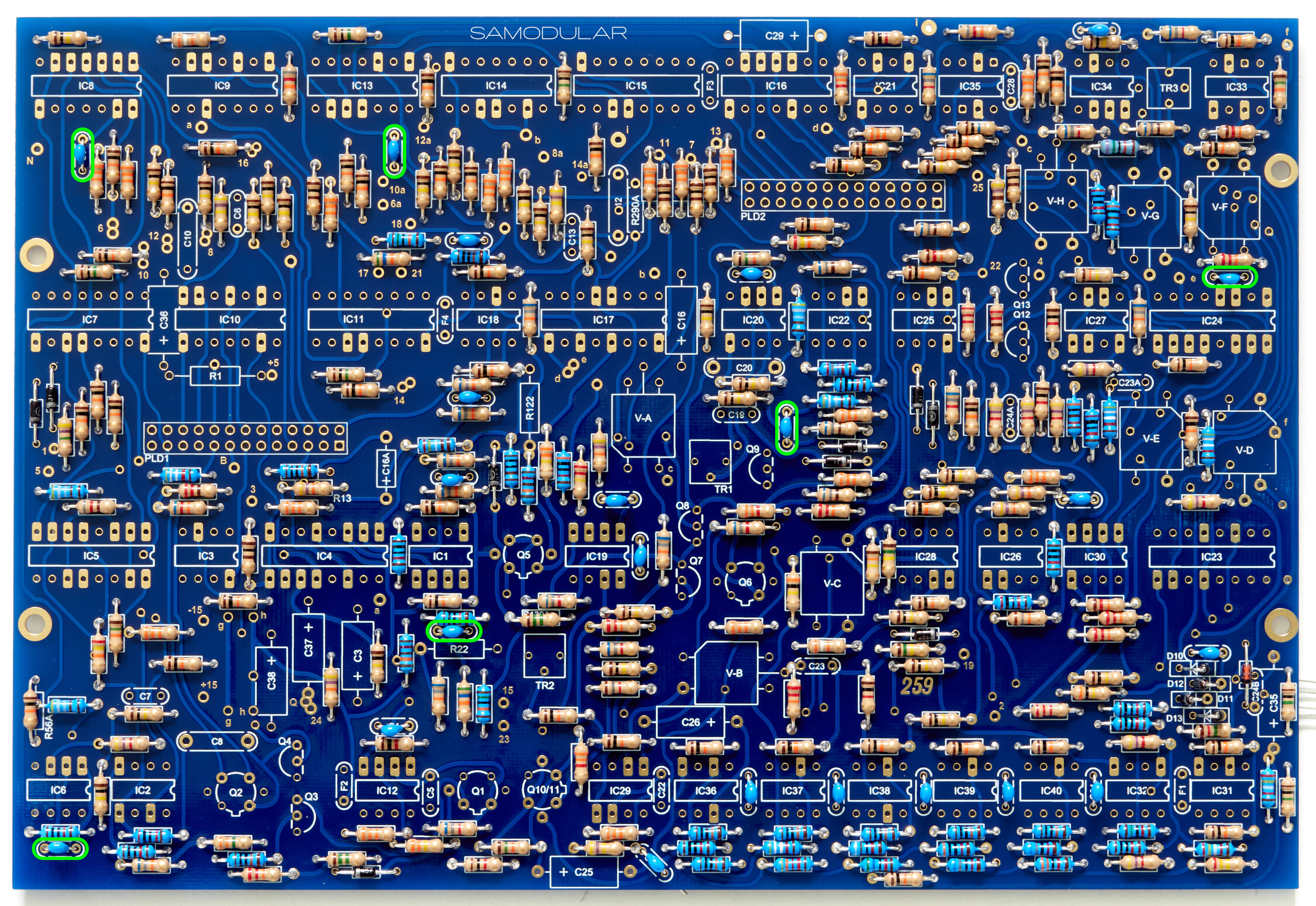
Placing resistors (100K – 13M)
Repeat the procedure from Part1 – now with 100K to 13M resistors.
Click on the thumbnails below for high resolution images.

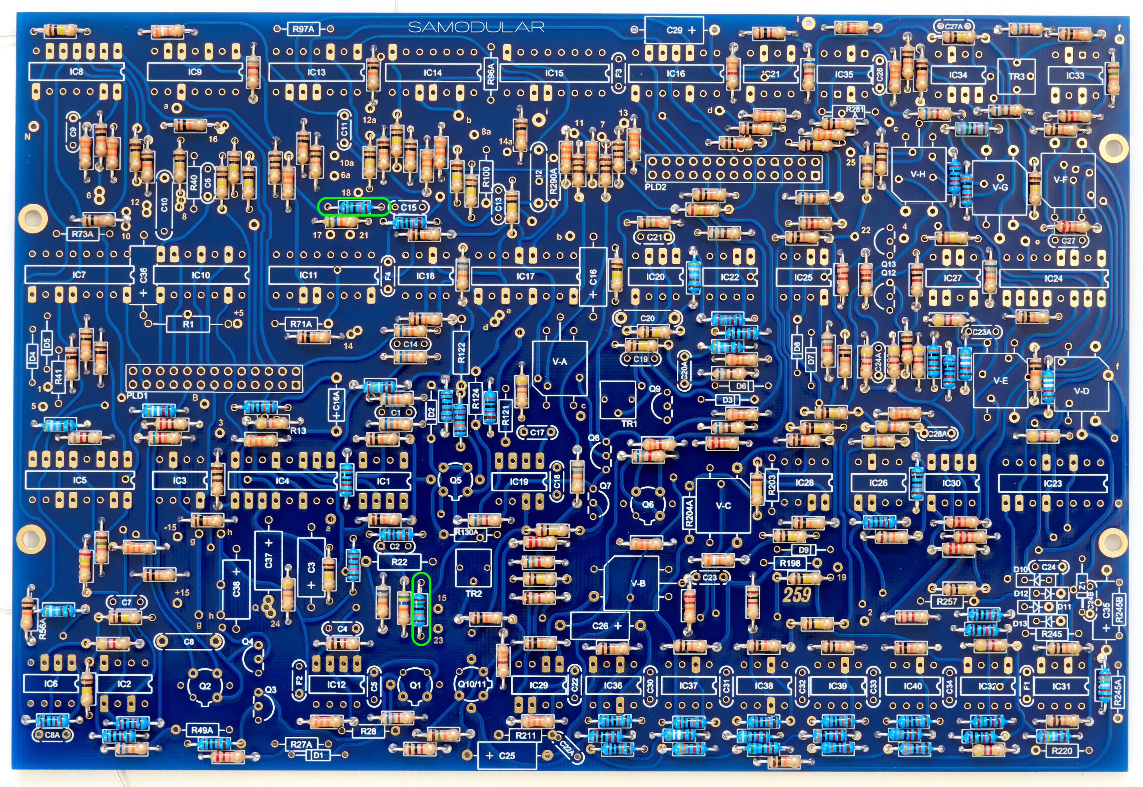

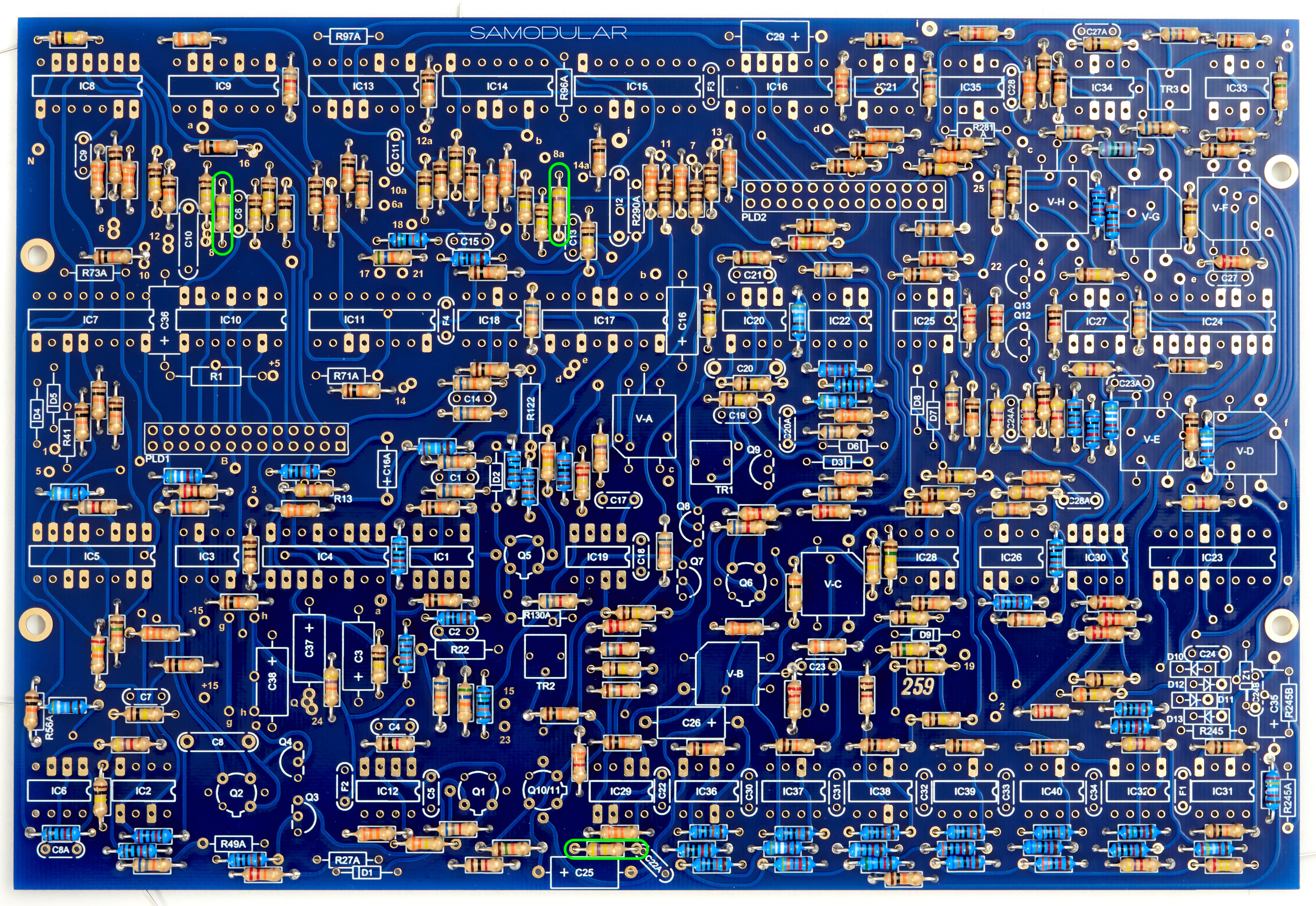

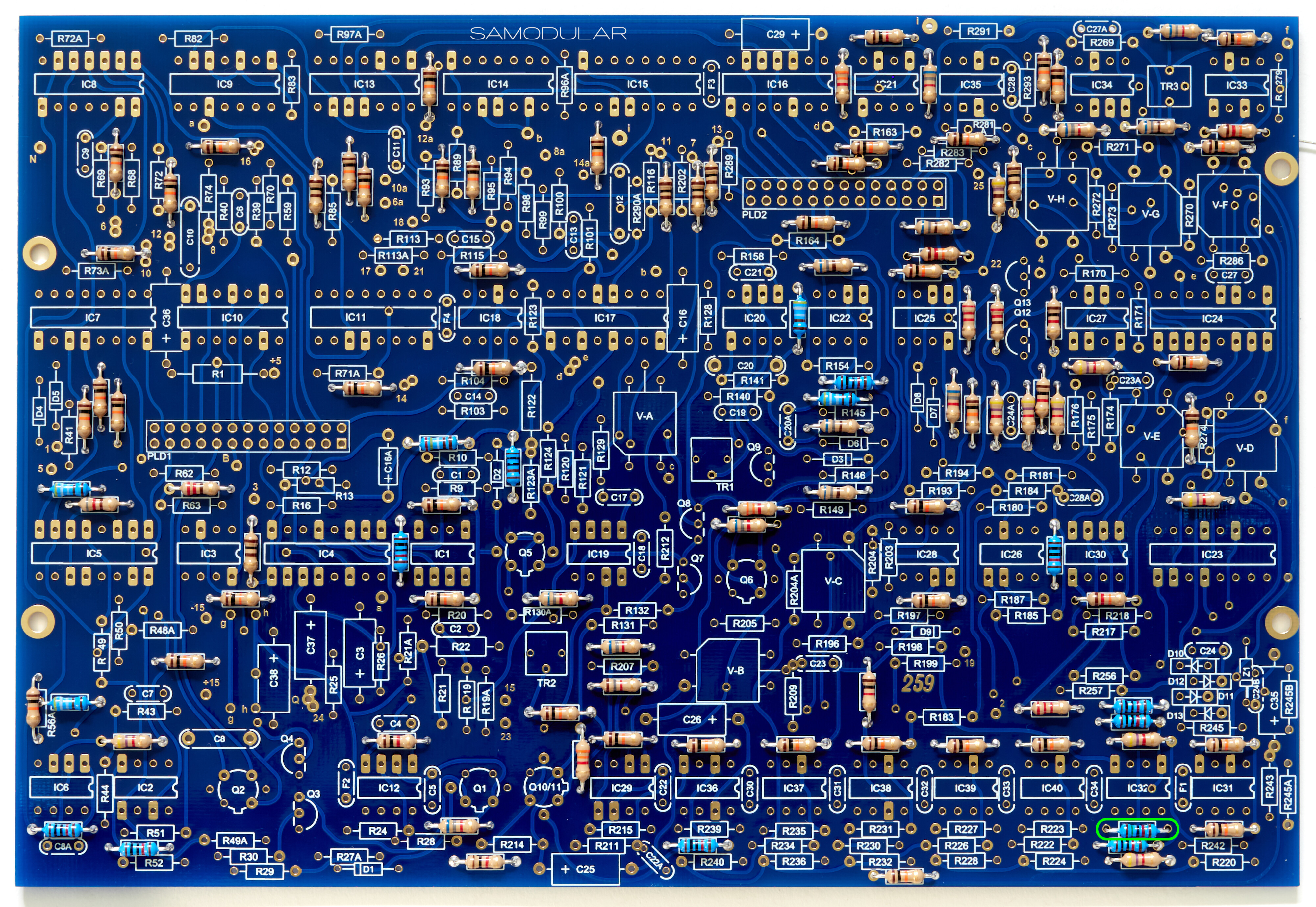
After soldering snip off all component leads and wash the PCBs. If you can proceed with the next step the same day – wash after Part 4.
Click on the pictures for high resolution images.
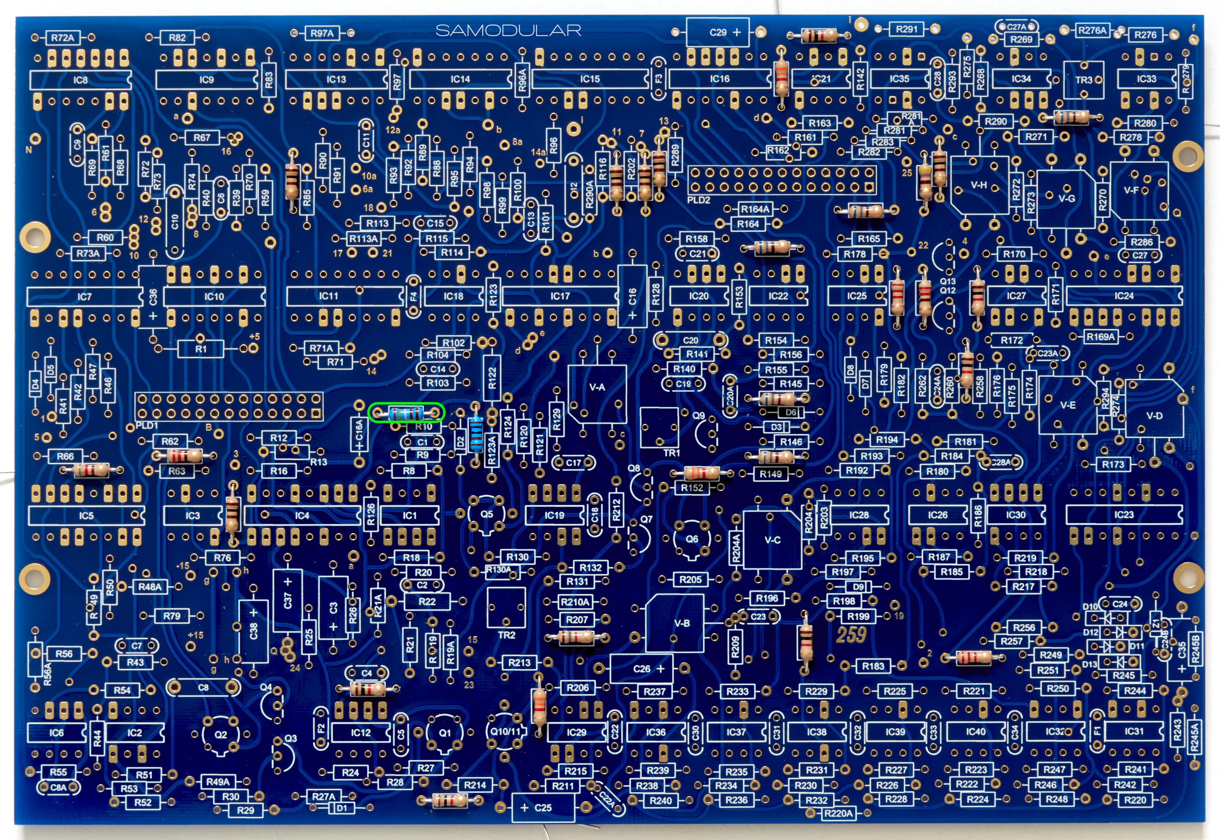
Part 4 – PCB2
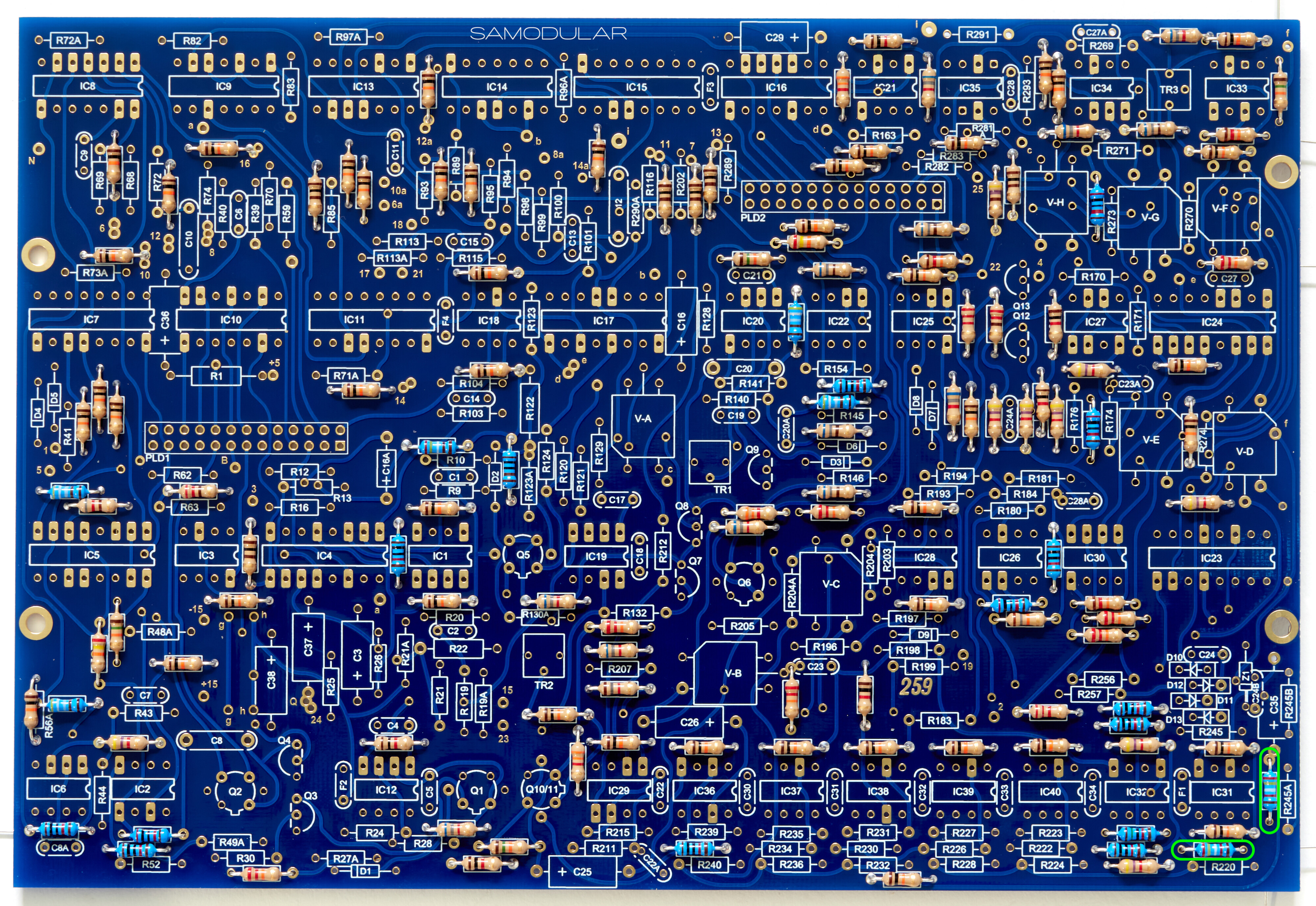
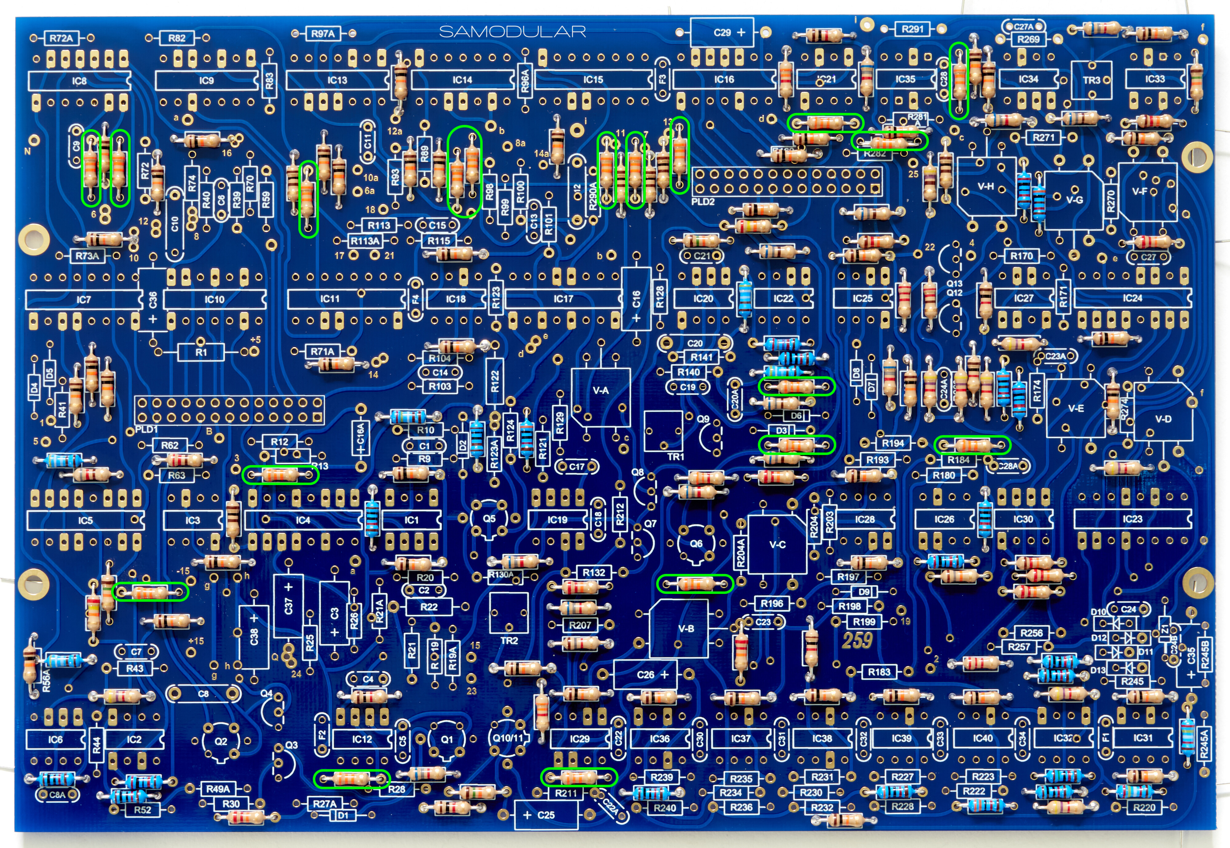
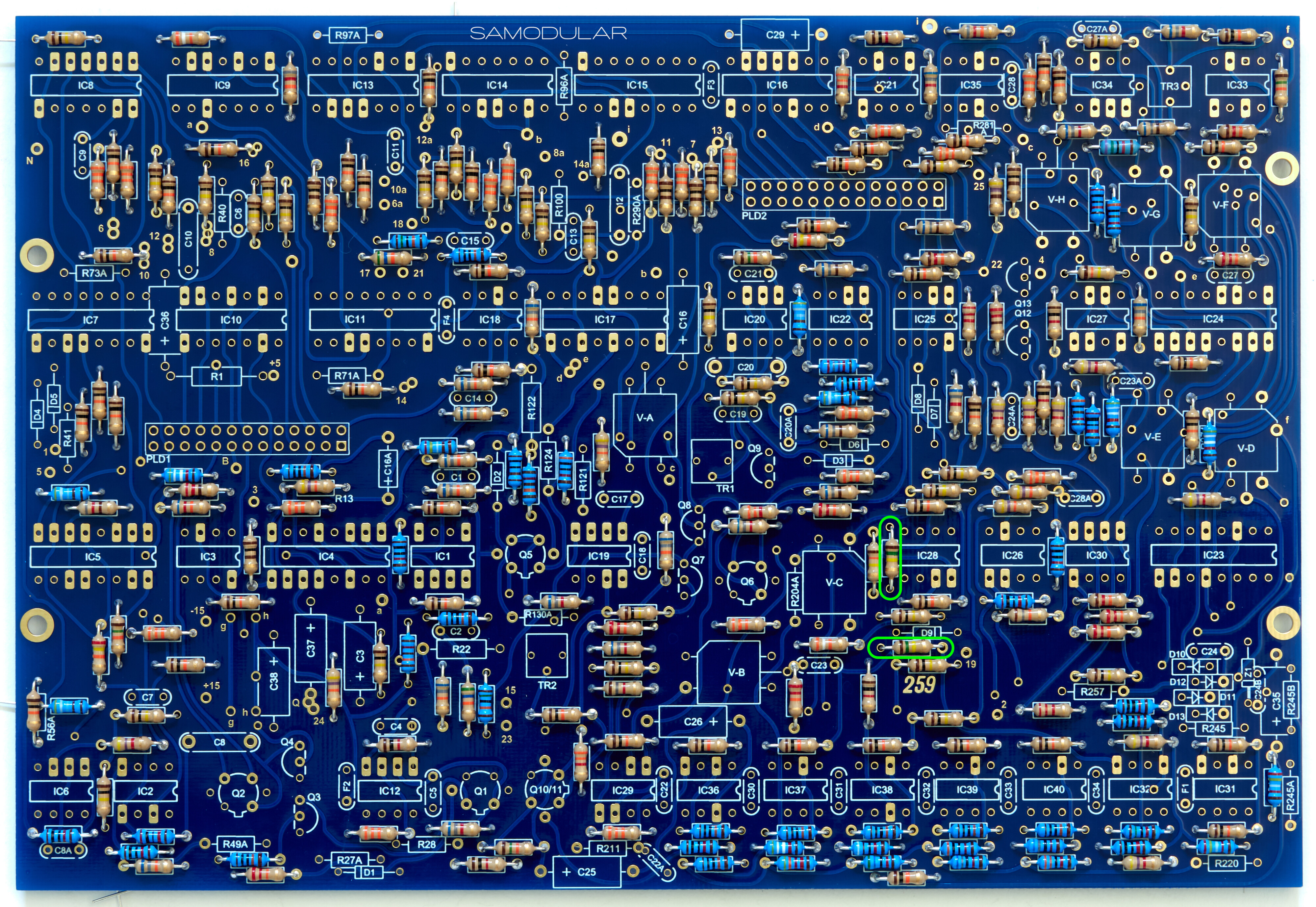
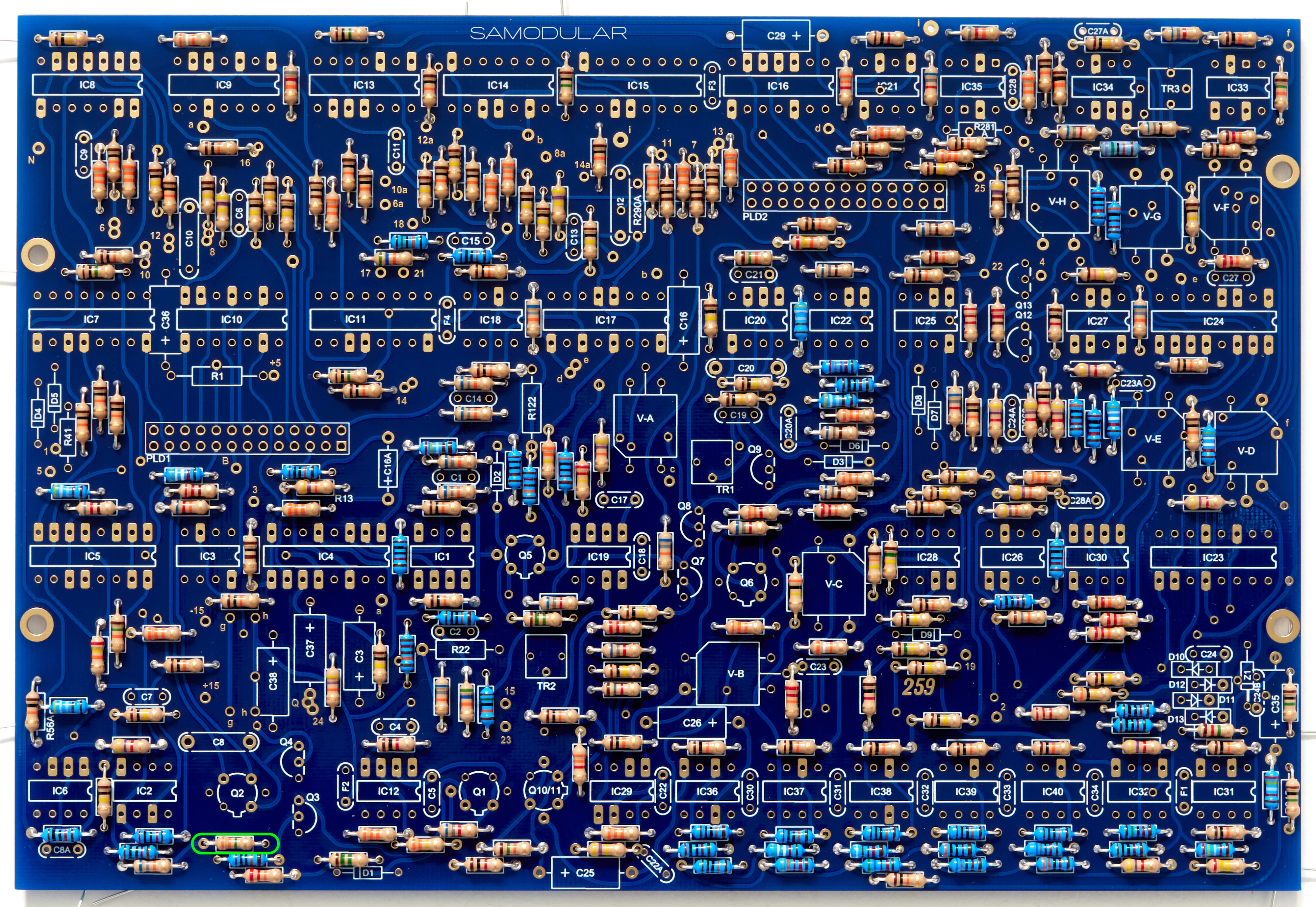
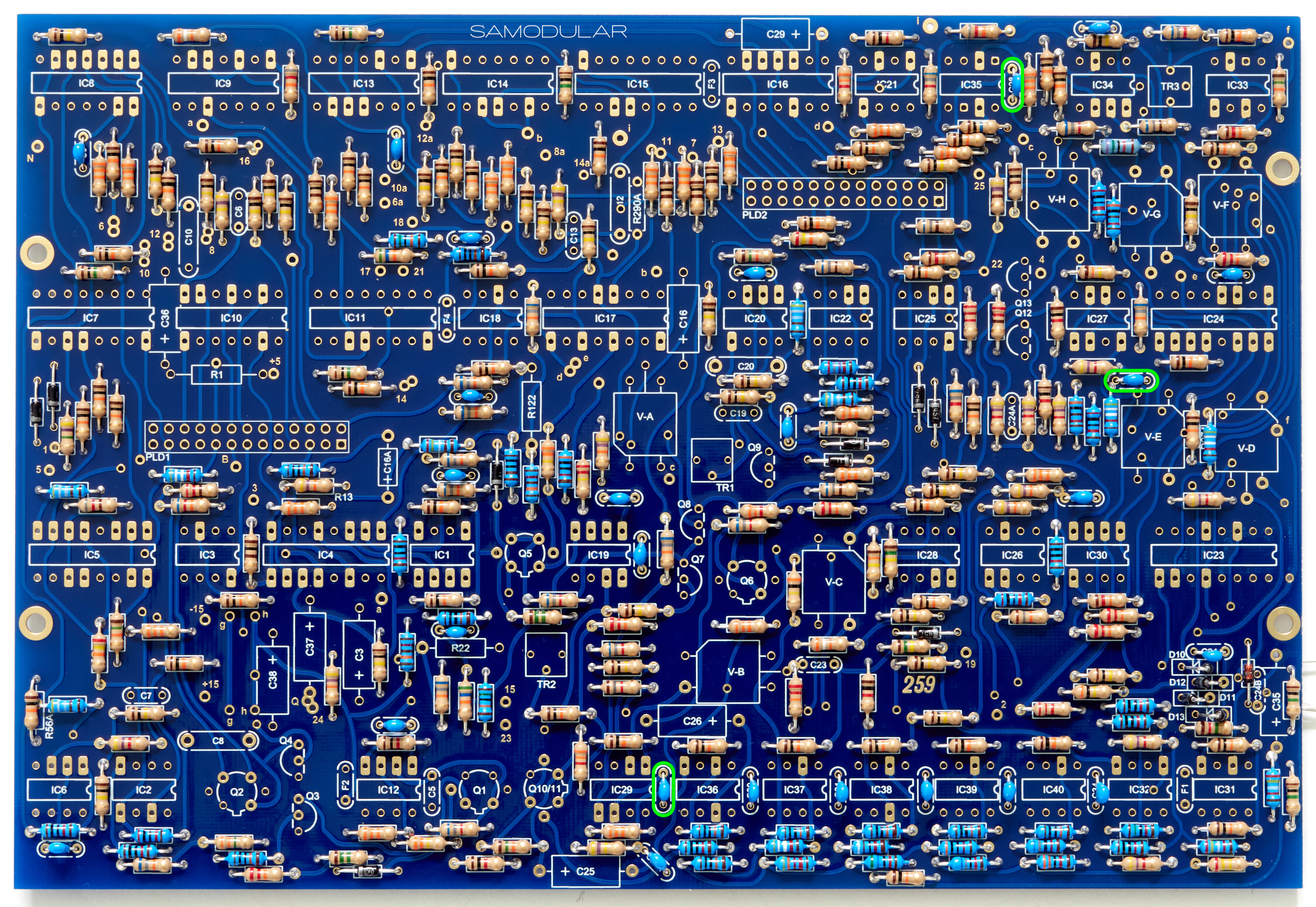
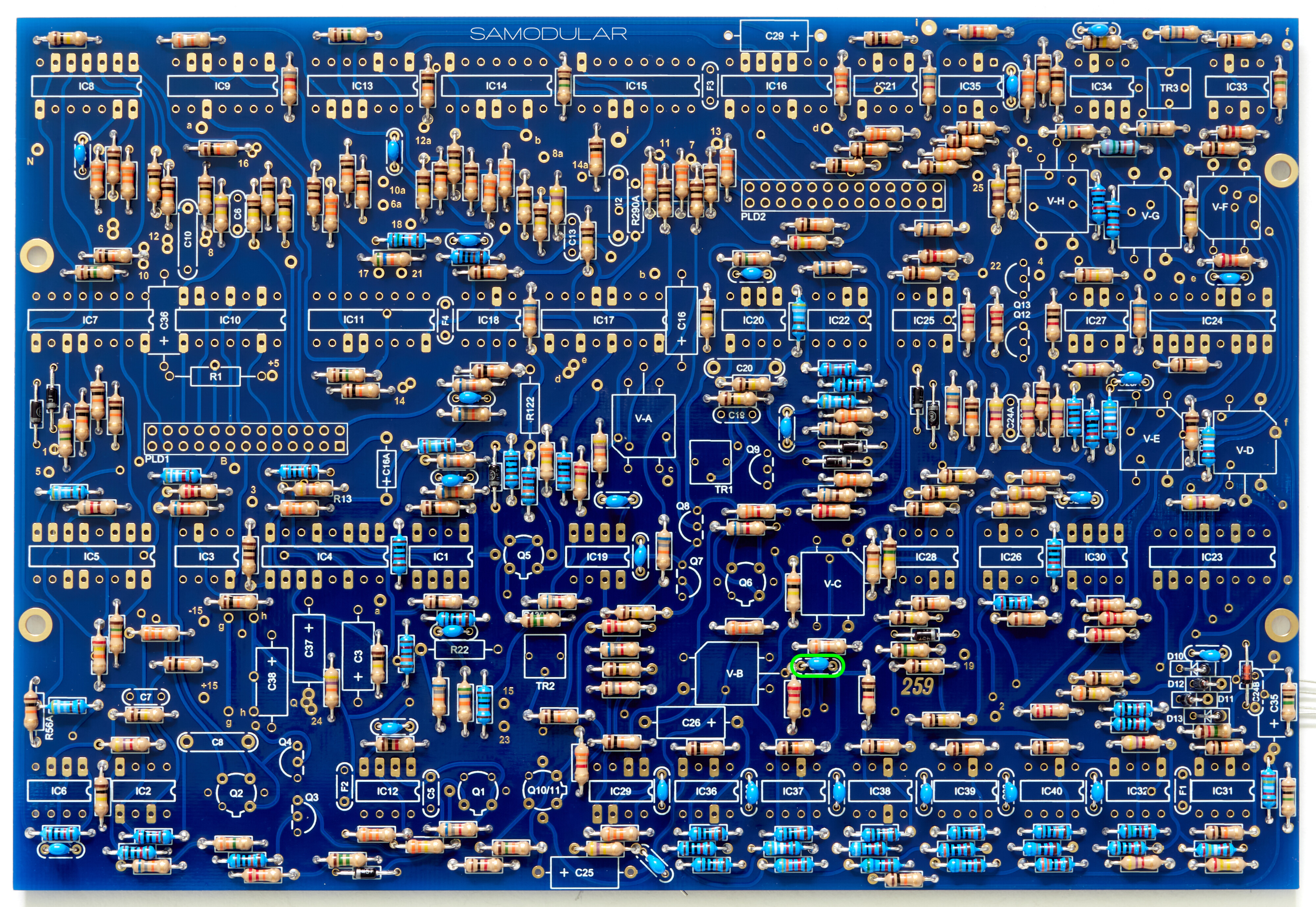
Placing diodes & capacitors
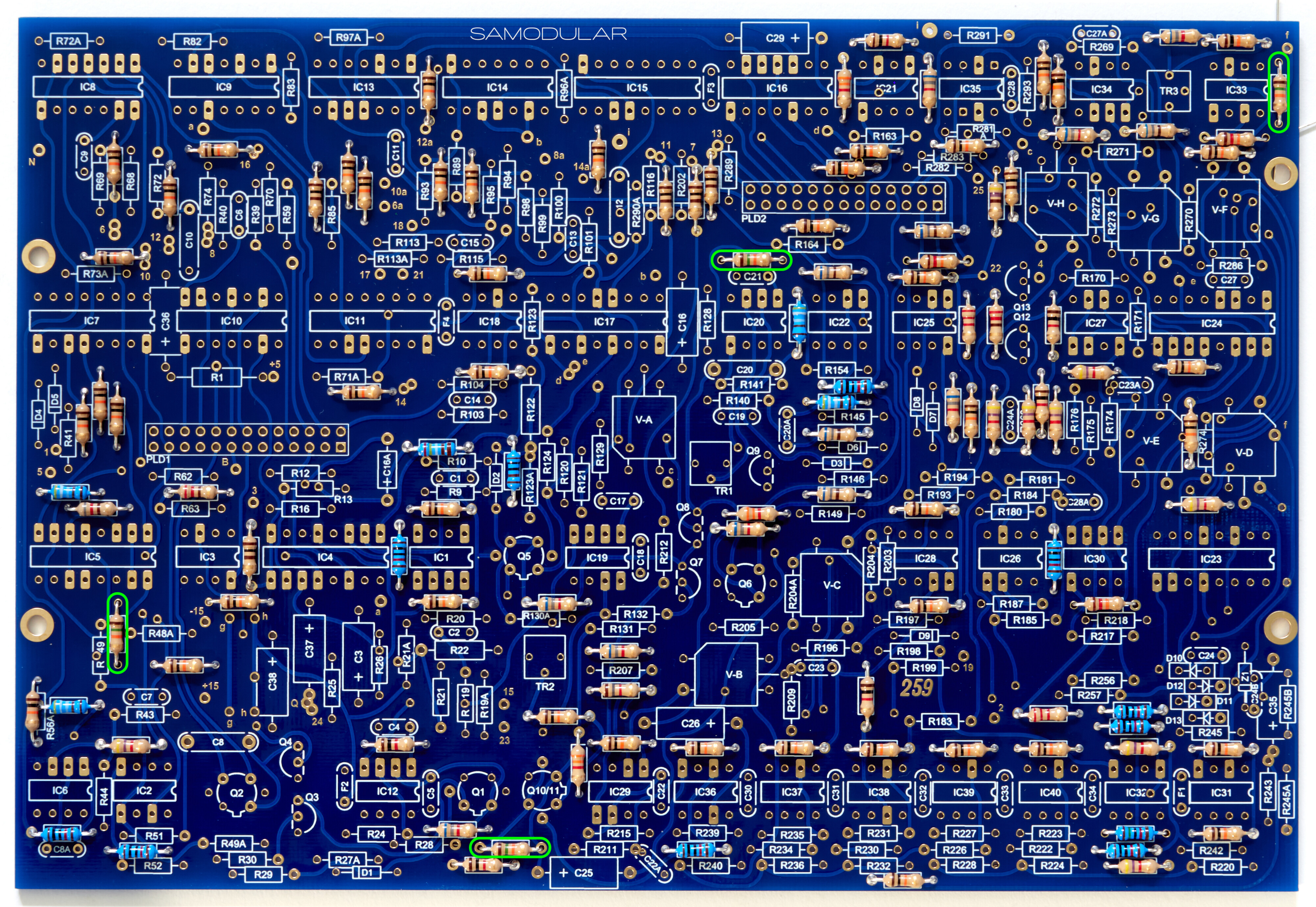
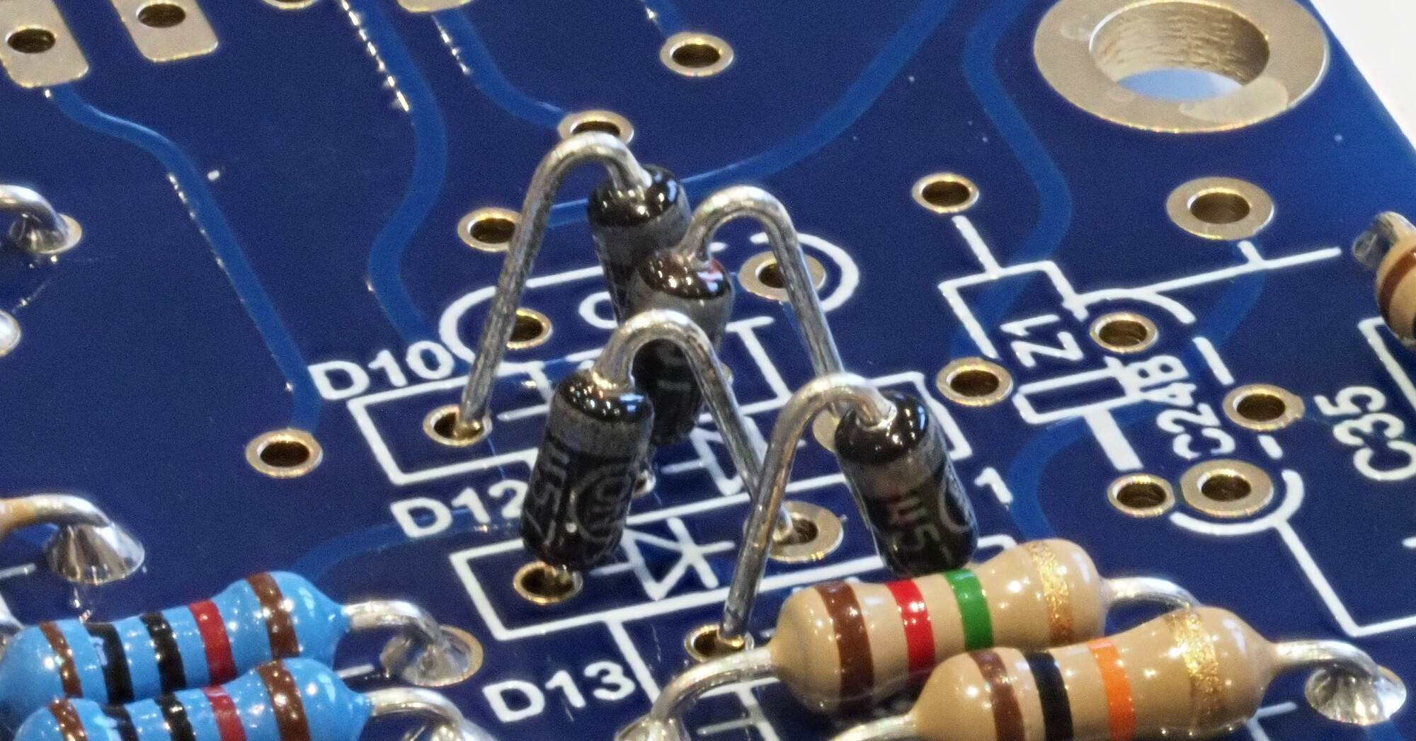
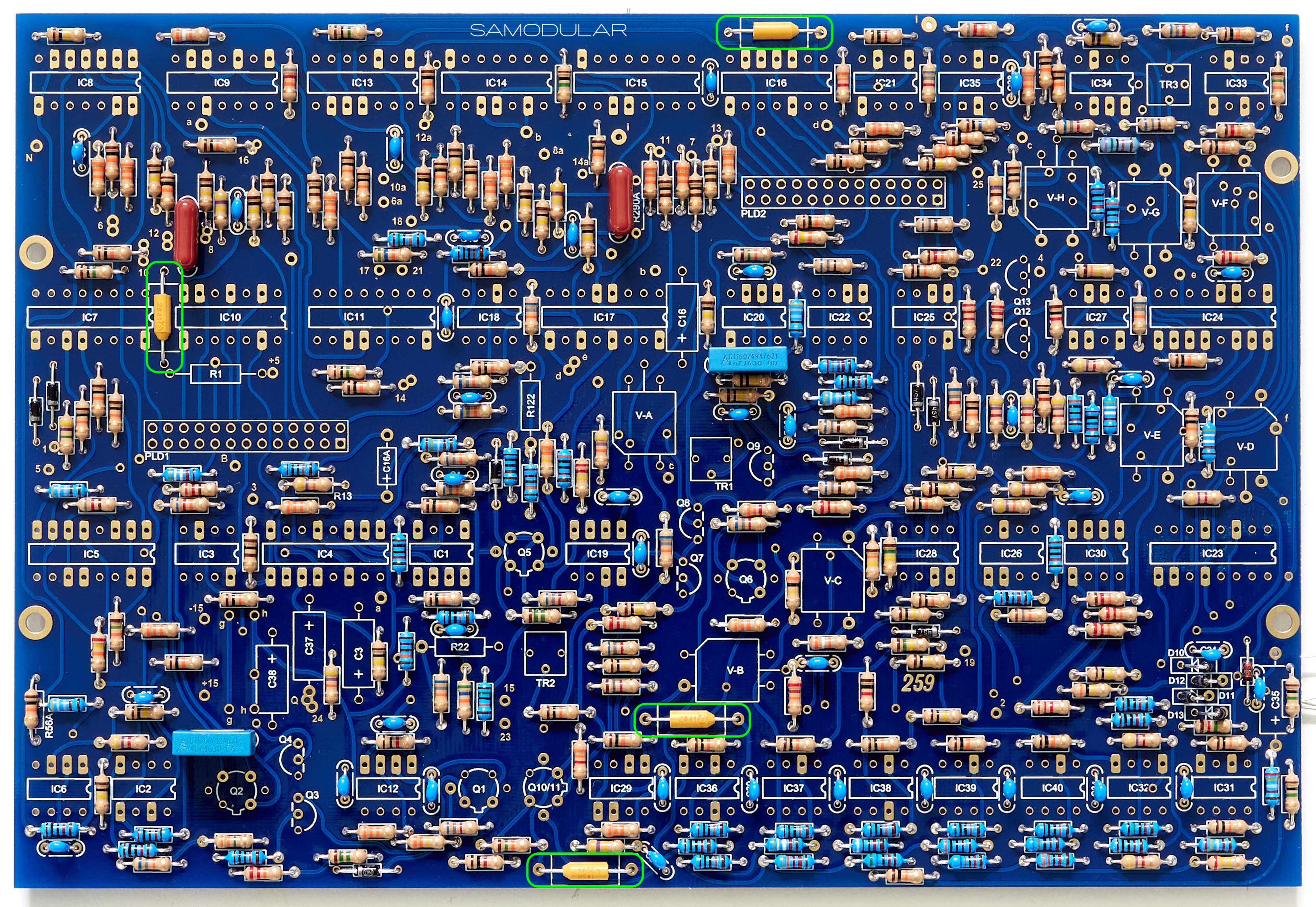
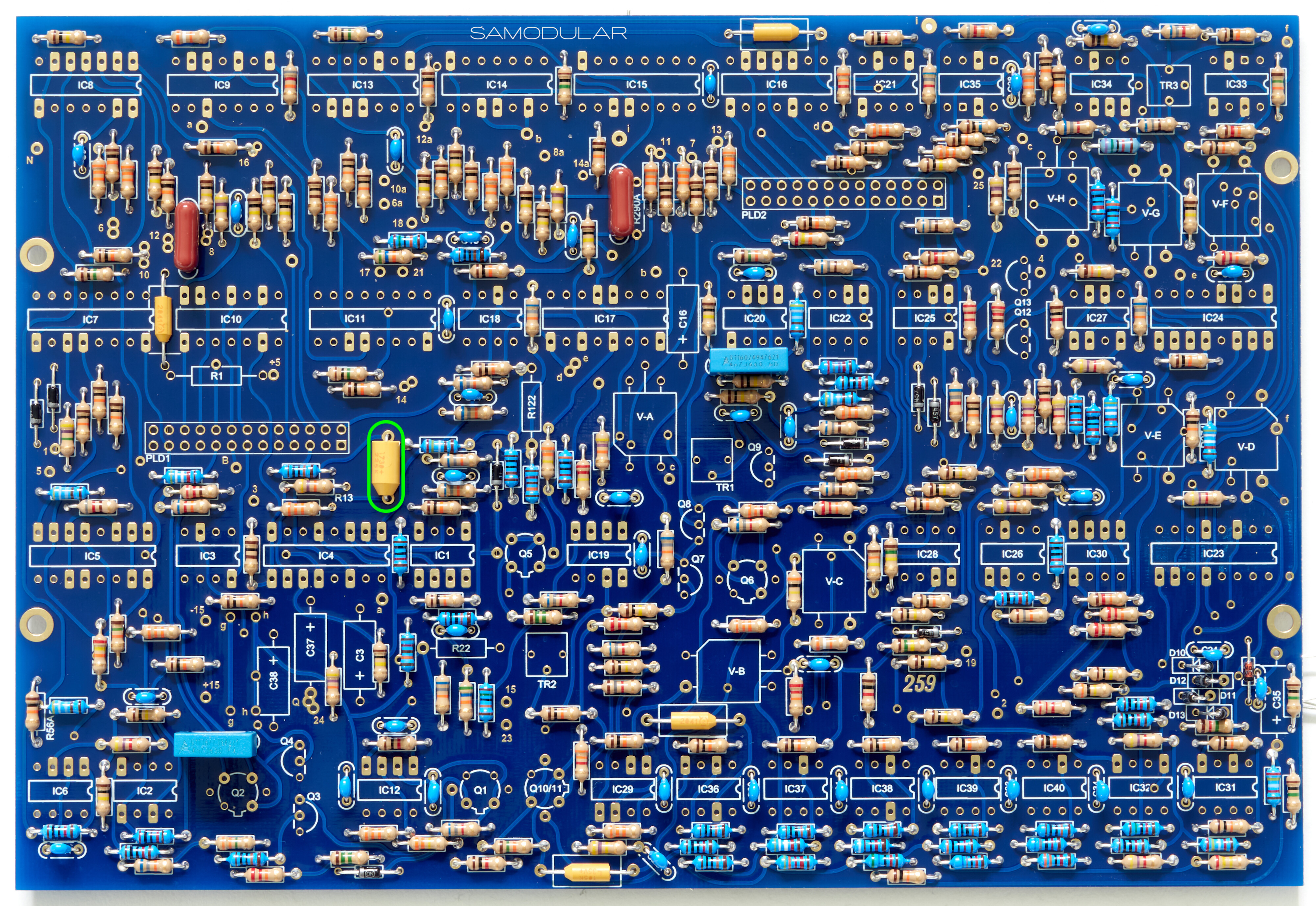
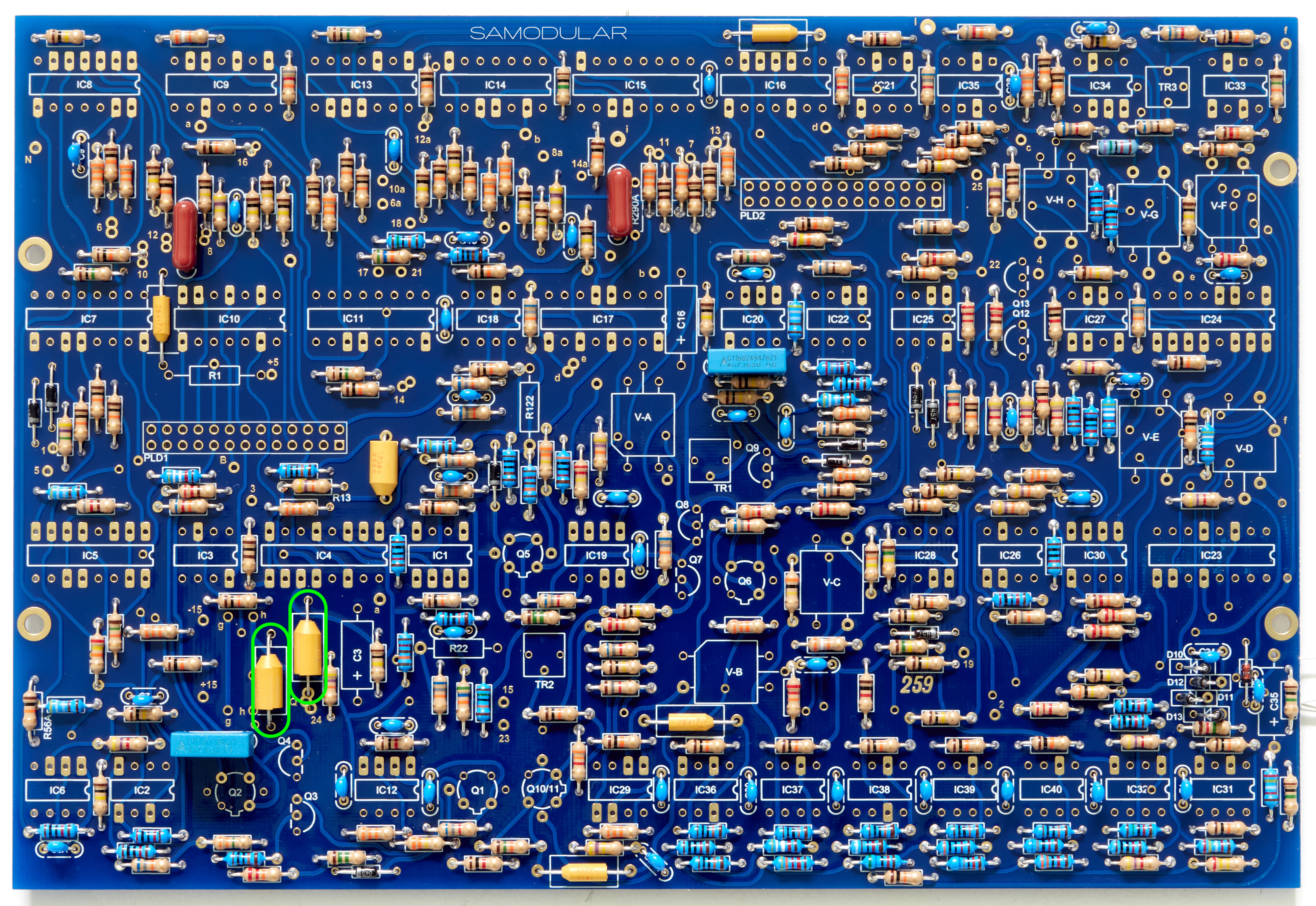
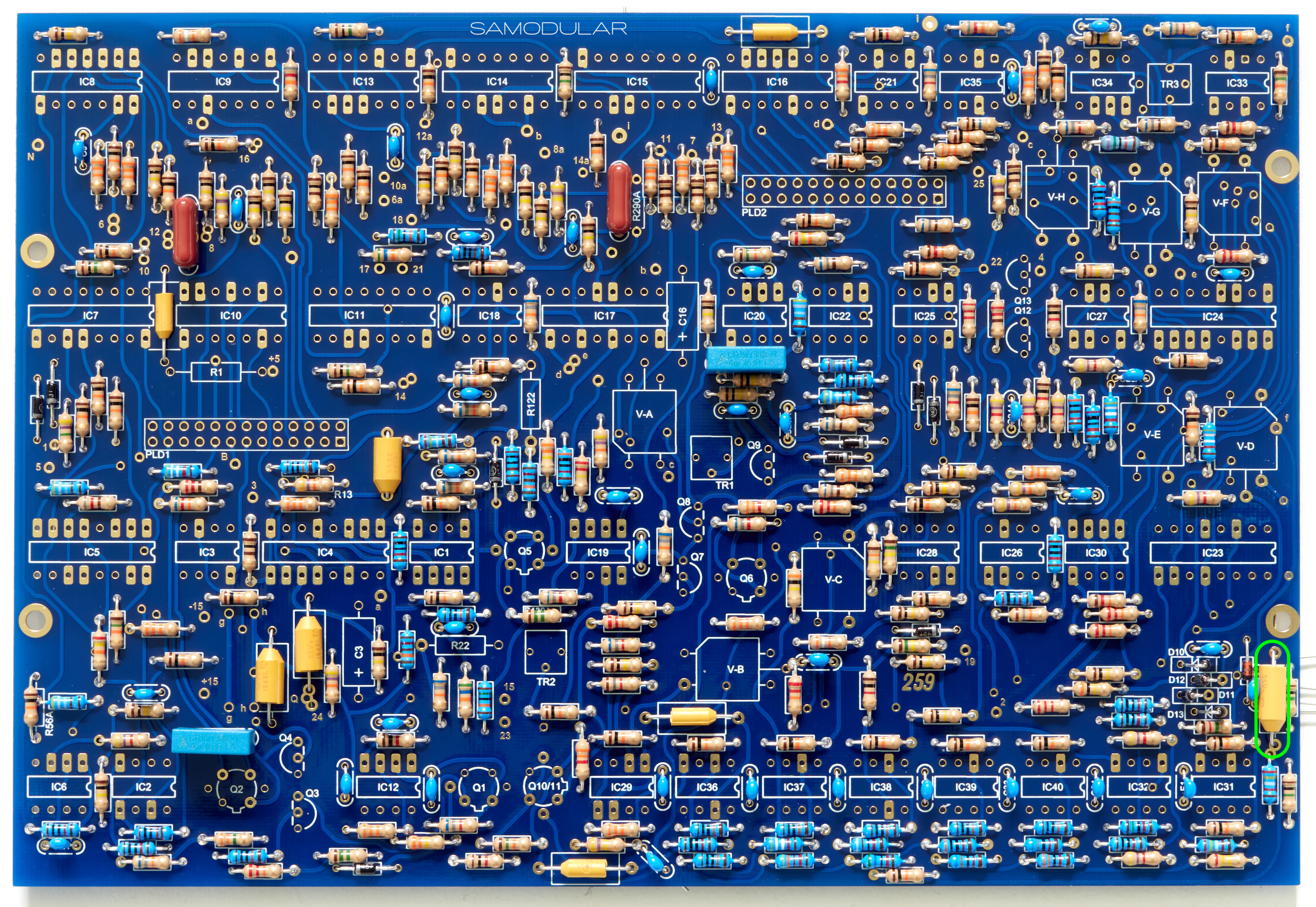
Repeat the procedure from Part1 – now with the diodes. Please note that the diodes have a different leadspacing – check before bending the leads. Please also note that you need to bend diodes for D10 to D13 differently. I just use my fingers to bend those.
Click on the thumbnails below for high resolution images.

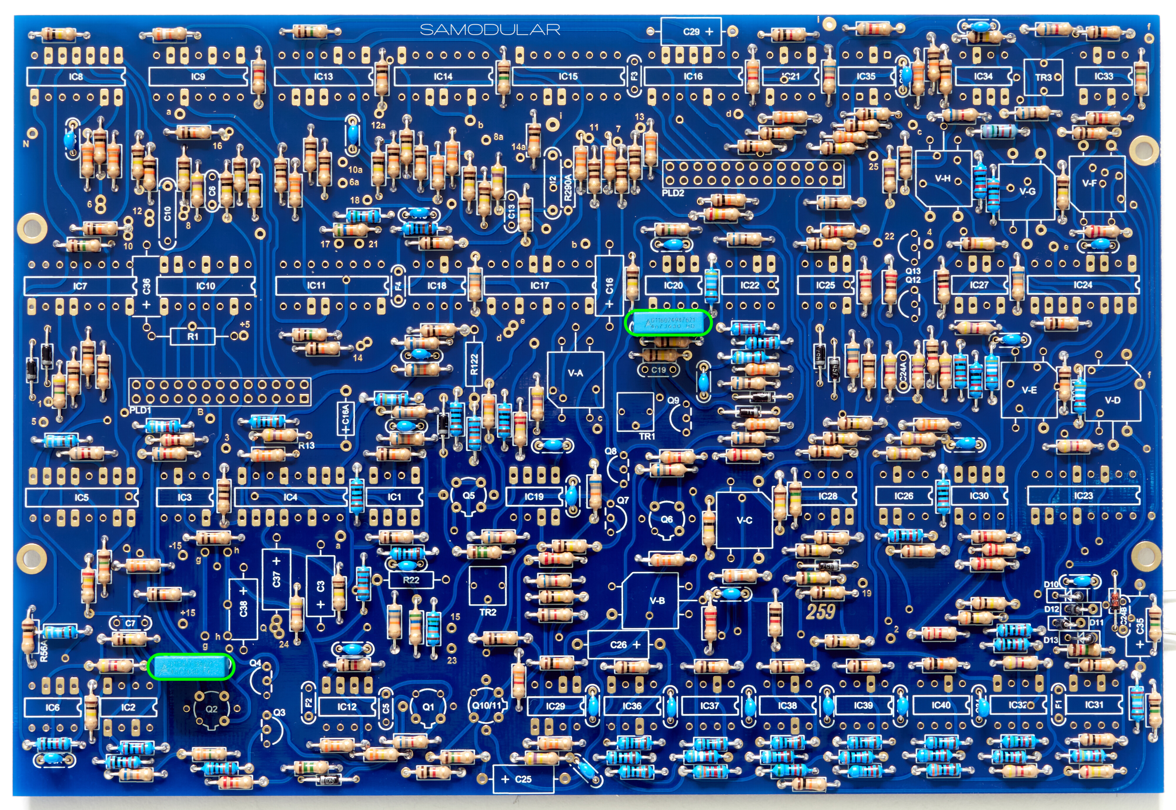

Congratulation 🙂 Allmost resistors and capacitors are in place – except the 1K Tempcos. I will install them later.
What did I forgot ? The 1R 1W resistor. Add it to R1.
Now lets move on to Part 5 – PCB2 Semiconductors
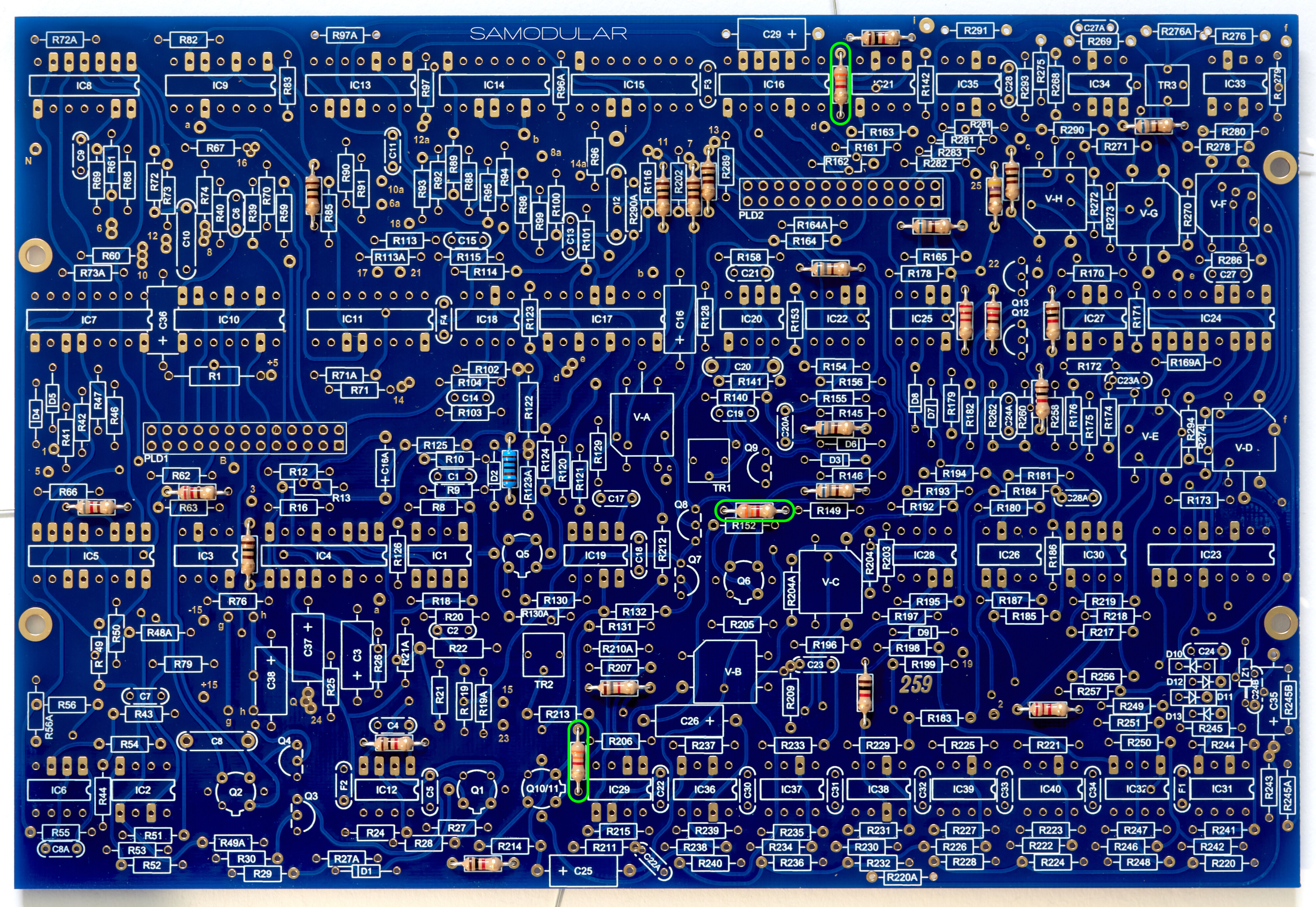
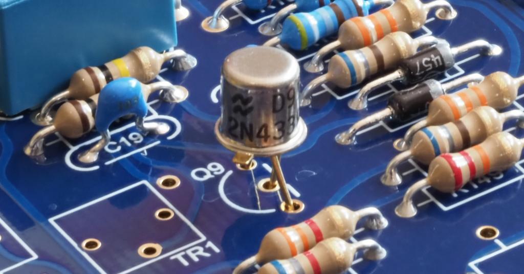
Part 5 – PCB2
Placing jfets / transistors
I will start with Q9 – the 2N4339. It is selected for an IDSS between 0.8mA and 1.2mA. This should give me a nice sine wave. You could also use a selected J201 instead. If you’re using a J201 just follow the silkcreen on the PCB for the correct orientation. If you use a 2N4339 please install as pictured below.
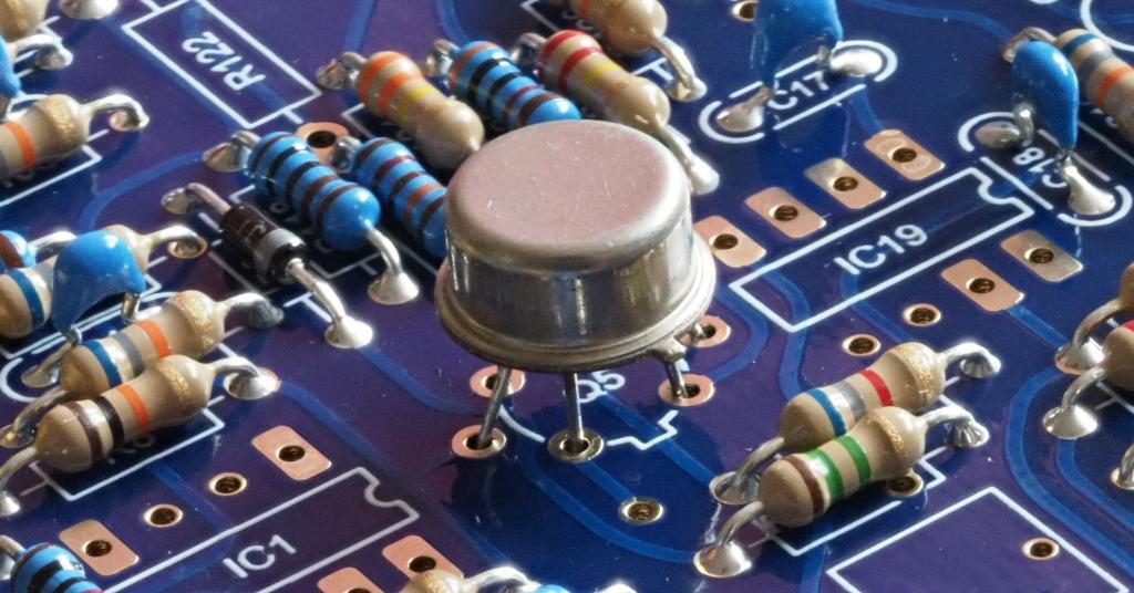
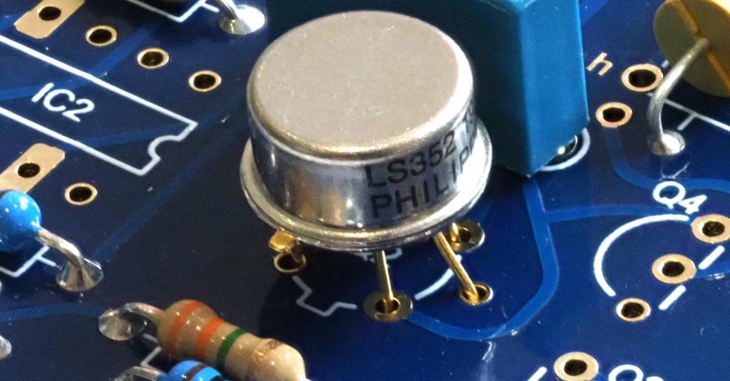
Next are the KC811 dual-NPNs (Q1 & Q5) and LS352 or 2N3806 dual PNPs (Q2 & Q6)
Nothing special here. I pushed them in place and left a clearance of about 6-8mm. Bend the leads on the solderside of the PCB and solder later.
Go ahead with the 2N3958 (Q10/11) and the PN3565s (Q3, Q4, Q7, Q8, Q12, Q13)
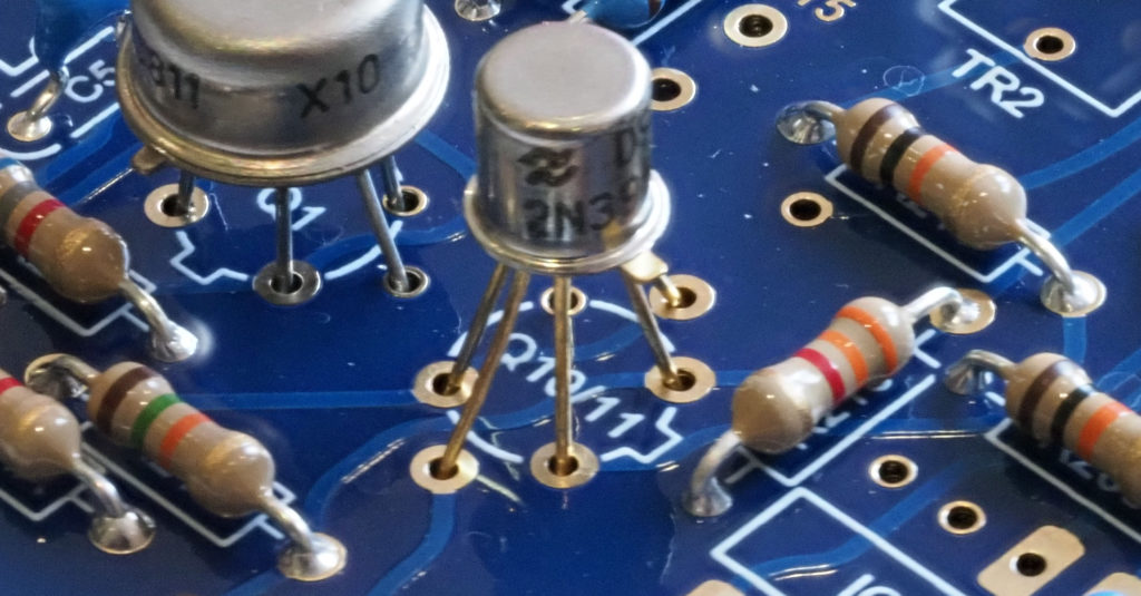
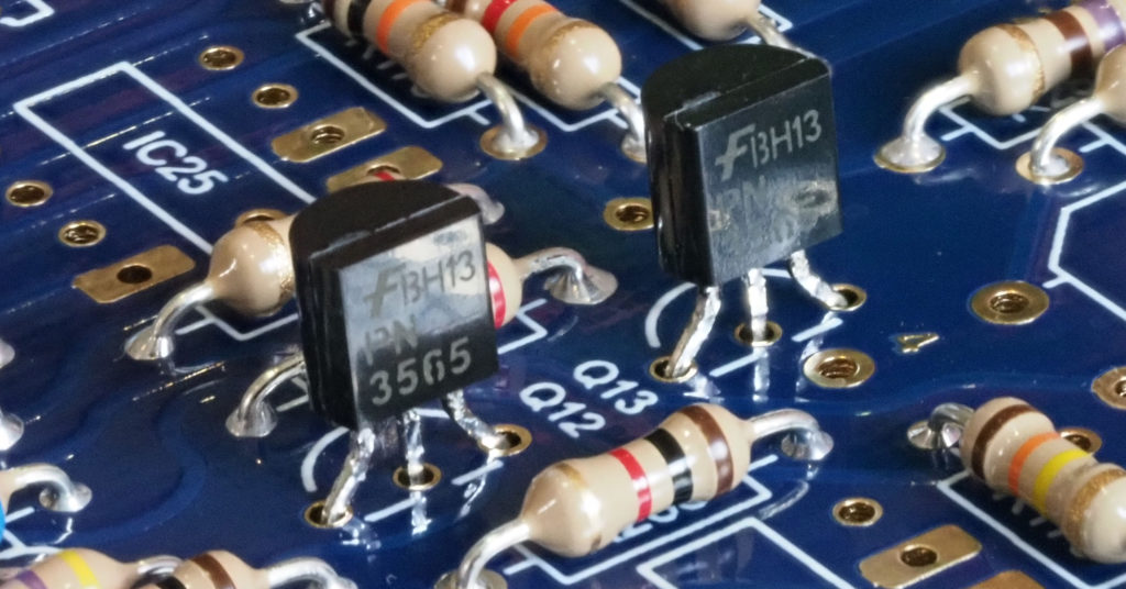
Please solder all transistors / JFets now. Make sure to solder only 1 pin of each component to avoid overheating ! Once you have soldered 1 pin of each component you can proceed with pin 2, then pin 3 etc of each component.
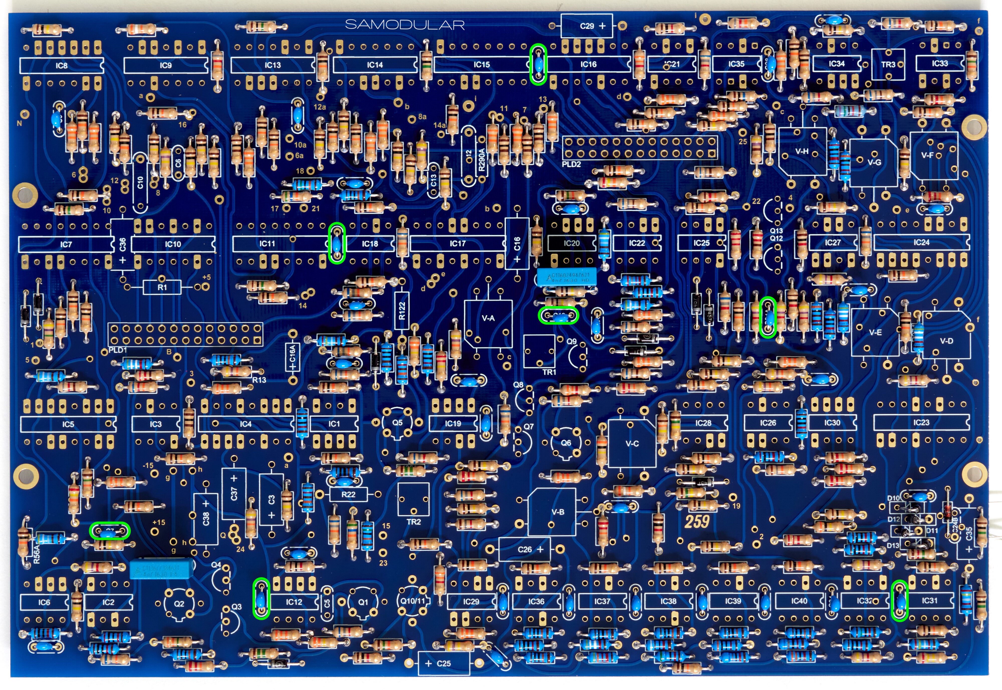
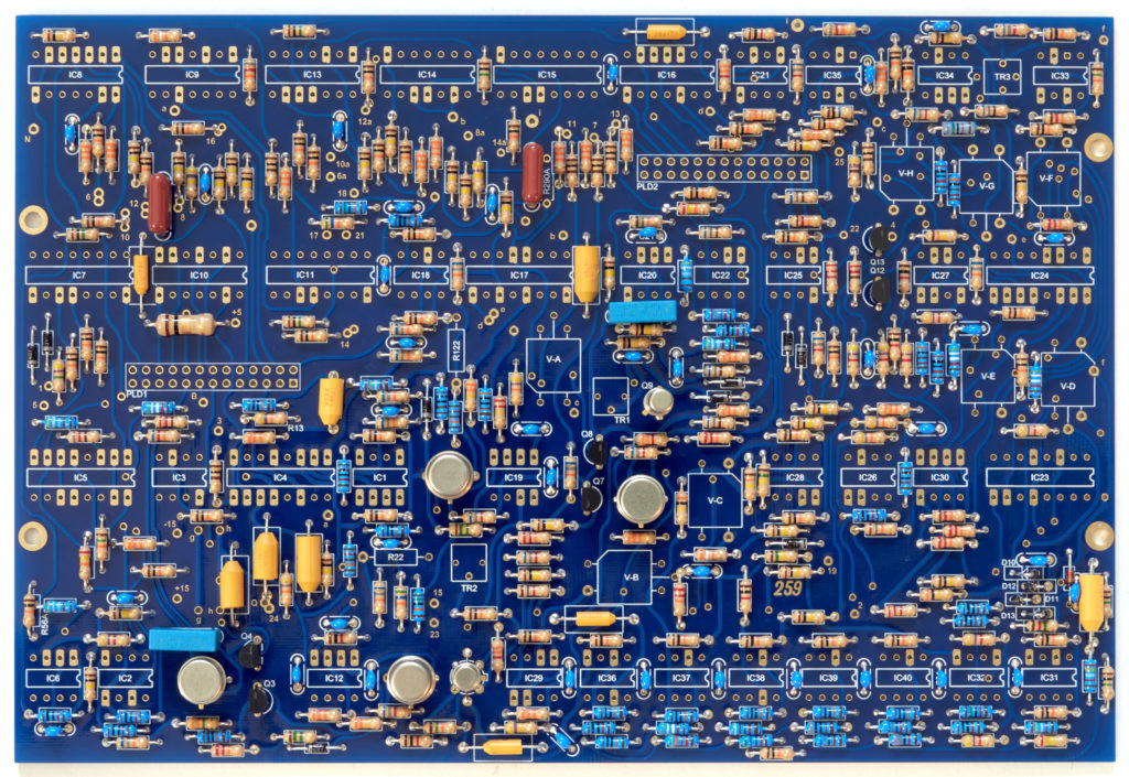
At the end of Part 5 your PCBs should look like this:
Part 6 – PCB2
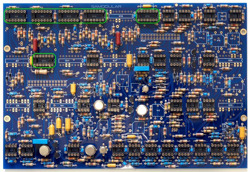
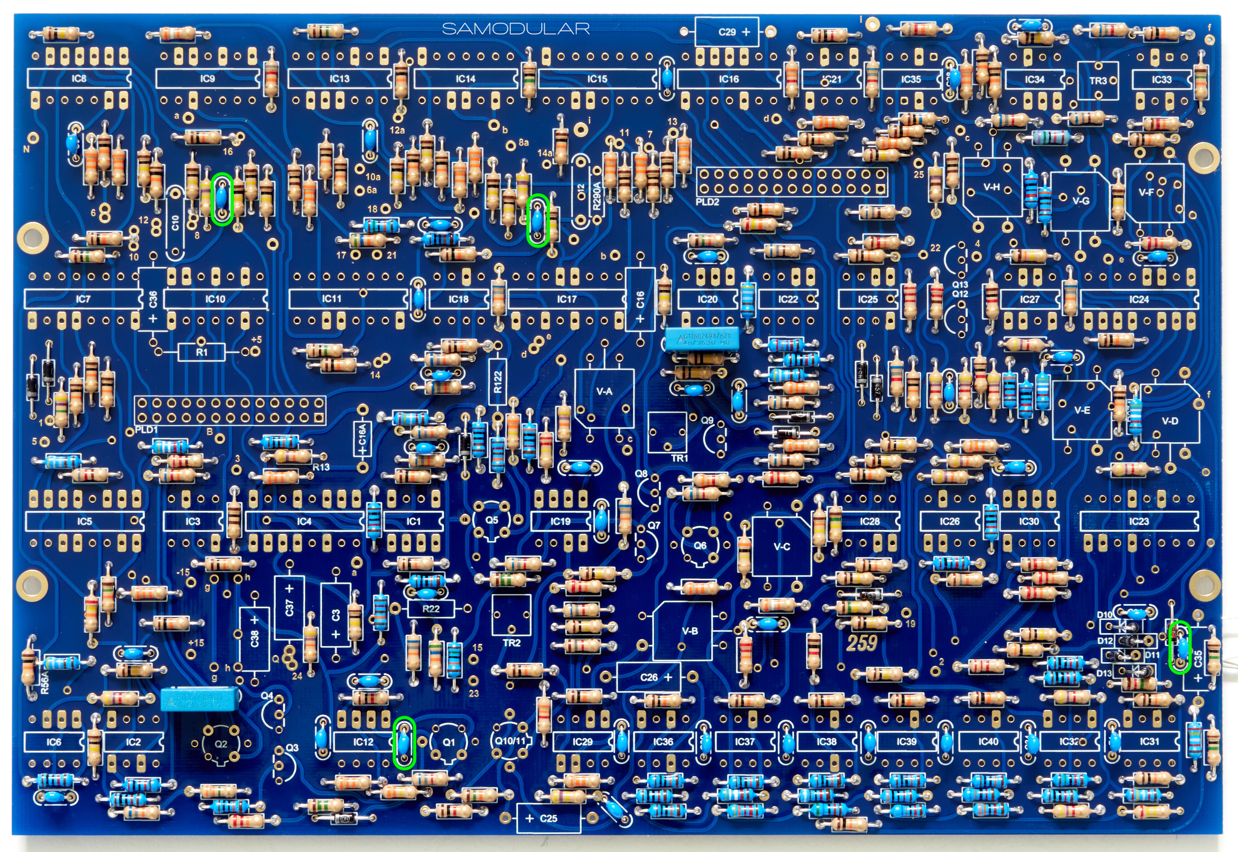
Placing DIP sockets
I will start with the 8-pin DIP sockets, then 14-pin and then 16-pin sockets. Solder just the first and last pin of each socket to hold them in place. When all the sockets are in place, flip the board and solder the remaining pins of all sockets using water soluble solder.
This is the last time water soluble solder will be used. Please wash and dry the boards thoroughly after this build step !.